ENGR338 Lab 2021 Spring
An 8-bit SAR ADC
Tyrone Bracker
tabrackeryazzie@fortlewis.edu
Final Report: The Successive Approximation Register Analog-to-Digital Converter
Introduction
Successive Approximation Register (SAR) is a type of
Analog-to-Digital Converter (ADC) that is used to return a voltage
value as closely possible to an orginal voltage input. The higher the
resolution/bits of the SAR ADC, the closer the approximate voltage
output is closer to the original voltage input; so a 4-bit SAR can
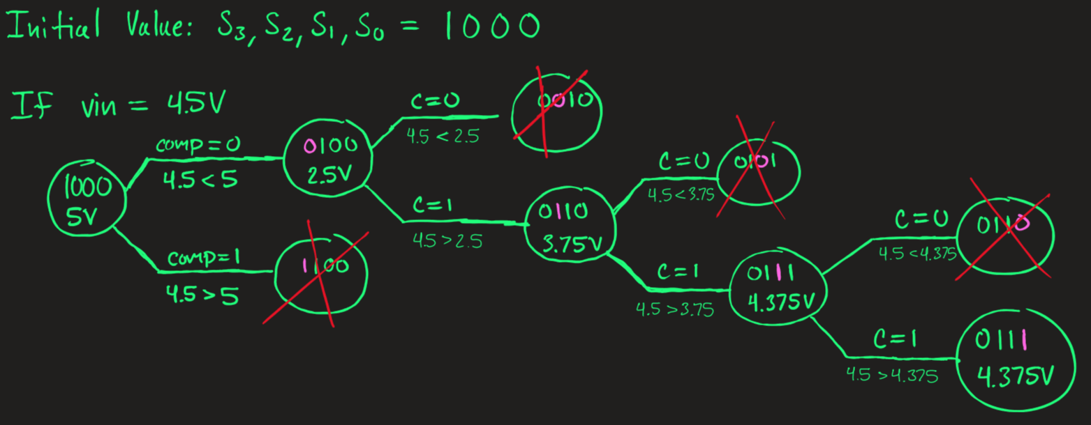
match a 4.5[V] input efficiently if the Voltage-Reference value is equal to 10[V] since the bits represent 50% of the entire voltage range.
Therefore, the bits begin at "1000", equaling 5 in decimal then working
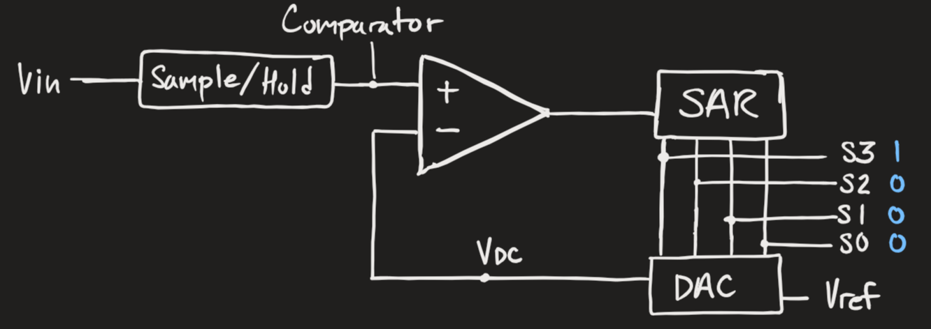
towards 4.5[V]. A drawn diagram of the ADC system can be seen below in
Figure 1.
Figure 1. Overall Structure of the ADC
The ADC process can be seen in Figure 2 with a total of 5 states
because there are N+1 states based on the N number of bits assigned to
the SAR. In this example, that N value is 4-bits, therefore 4+1=5
states.
Figure 2. SAR ADC example with Vin=4.5[V] and the final approximate voltage output being 4.375[V]
The maximum amount of voltage our 4-bit SAR ADC can handle is aroud
10[V] since the max bit value is "1111" which is 9.475[V] for our
example and based on the 10[V] 'Vref' value. To improve the accuracy we
can increase the bits from 8 to 18-bits. For this project I started
with a 4-bit SAR ADC to understand the system and worked on creating an
8-bit SAR ADC.
Materials and Methods
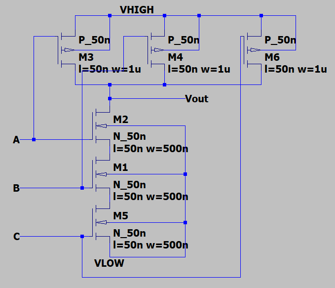
This
project began by making sure my NAND-3 Gate schematic was outputting
the correct logic with the given technologies. My initial length and width
values for the PMOS and NMOS were not the same as the ones in the
tutorial so once I saw those I shifted my values. I'm assuming that
these values come from the back of Dr. Baker's book because I had way
different values and wouldn't of thought to use 500 nanometer for the
width of the NMOS. The schematic for my NAND-3 gate can be seen below
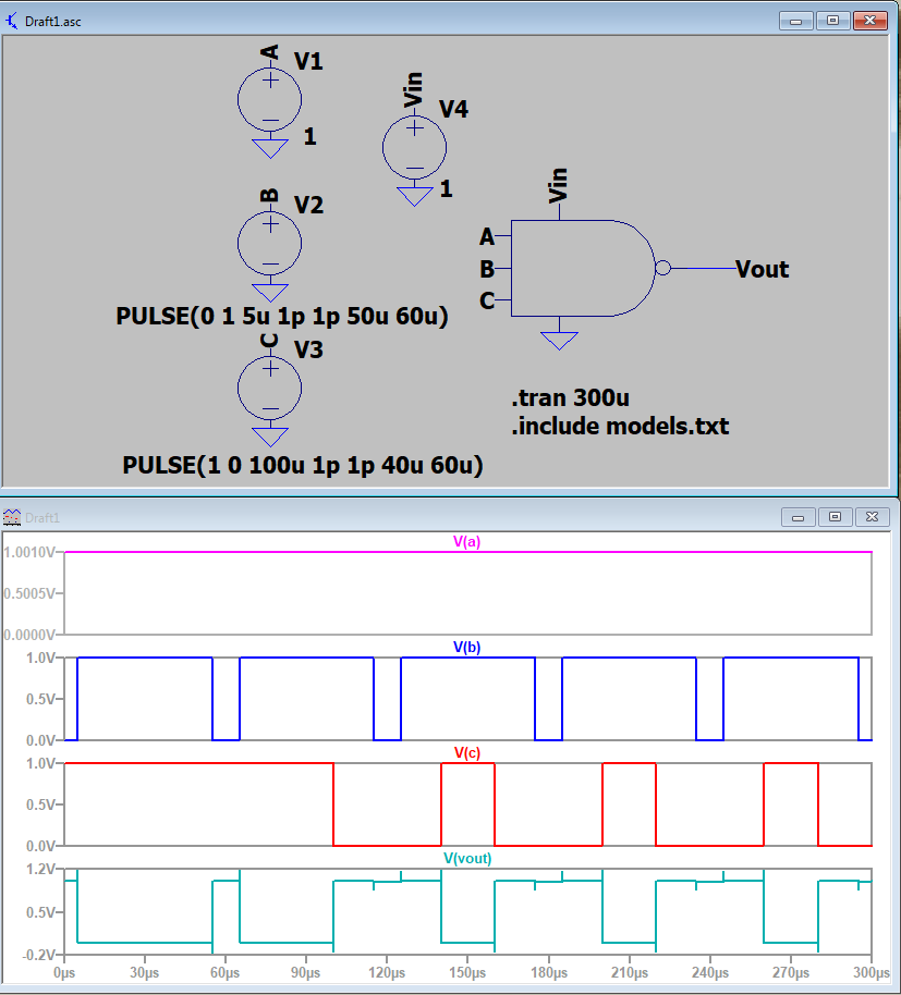
(Figure 3) along with a simulation (Figure 4) run afterwards to prove the logic was correct.
Although Figure 4's 'vout' is slightly noisey, the correct output is
displayed when all three inputs (A,B,C) are '1', equalling '0'
for the output and when ever any of the three inputs are '0' the output
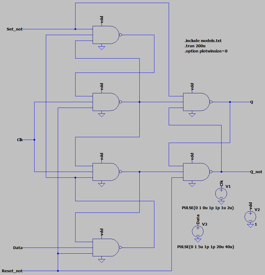
is always '1'. From here the Texas Instrument D Flip-Flop (TI DFF) was
developed using multiple NAND3 gates which was converted into a symbol. The TI DFF schematic was made and run
through the same tests as the NAND3 gate before it, by simulating and
making sure the logic was correct. The schematic (Figure 5) itself can
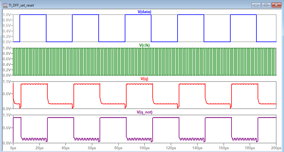
be seen alongside the waveform (Figure 6) produced from the simulation.
Figure 5. TI DFF simulation
schematic
Figure 6. TI DFF simulation
waveforms
As shown in Figure 6, V(q) and V(q_not) does a decent job at mirroring the V(data)
input, albeit with some noticable noise. With the correct logic, the TI
DFF was converted into a symbol and used in the next schematic for the
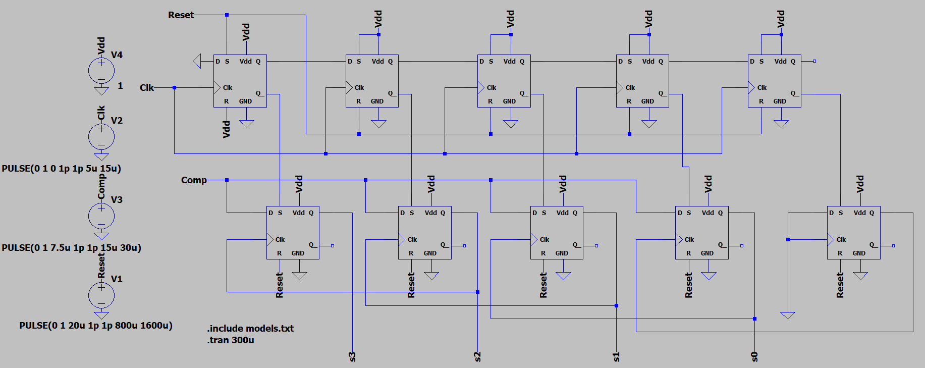
4-bit SAR ADC schematic. The schematic took on a row/column-structure with five TI DFFs on top and bottom. The bottom set acted as a sequencer and the top as a shift register. This structure can be seen in LTSpice in Figure 7.
Figure 7. SAR_ADC schematic
During the simulation I grounded the left over Q_ outputs
on the sequencer row which messed up my results. I would later
understand that this is because the TI DFF feeds that value back into
other NAND3 gates thus zeroing out different outputs. Eventually I did
manage to successfully simulate the SAR ADC by leaving those outputs
empty. Those results can be seen below.
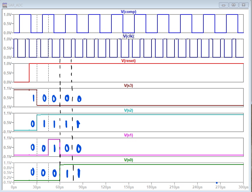
Figure 8. SAR ADC simulation results
The results read from top V(s3) to bottom V(s0),
so the first results are "1000", second is "0100", until the last
result "0101". The main focus is that during each rising-edge trigger
(dashed-lines),
the '1' shifted right from S3 to S0, which means our SAR block can
successfully shift the comparators values in the system. To finish this
4-bit design, it was converted into a symbol, simulated, and produced
results that mimicked Figure 8's, thus prompting me to
move onto the 8-bit SAR ADC design.
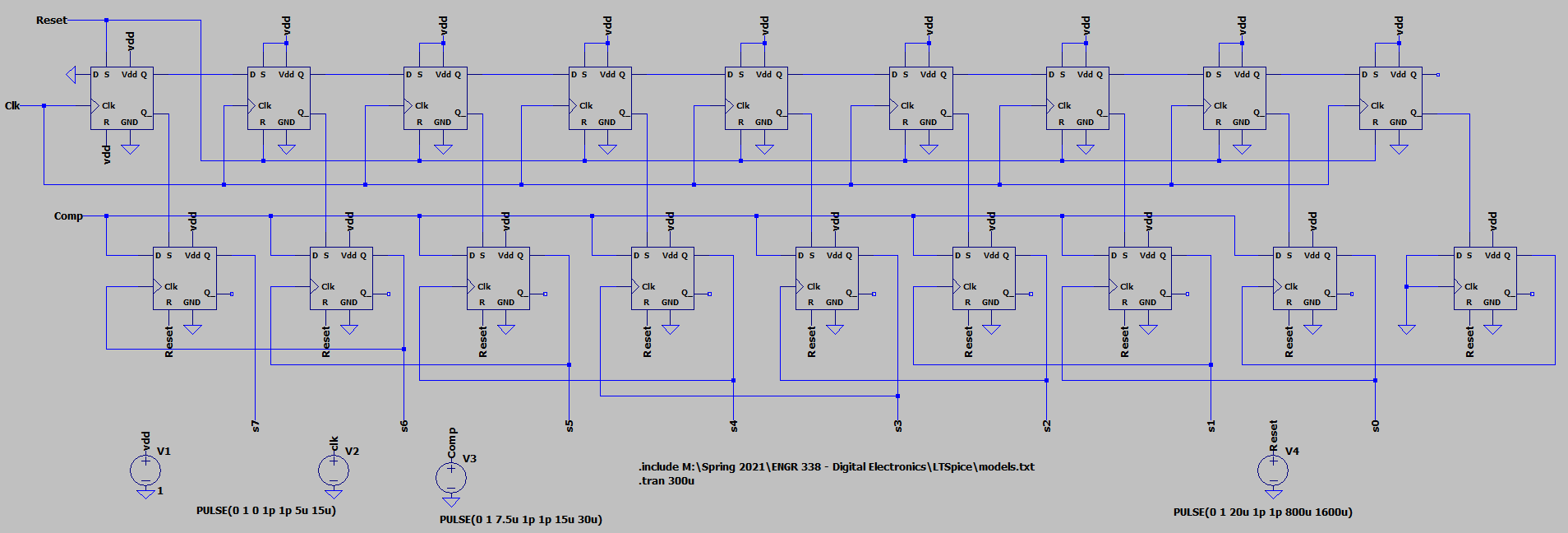
The 8-bit SAR ADC design was straight-forward to
implement because of the pre-established 4-bit design. The first step
taken was adding four TI DFFs to the sequencer as well as to
the shift register. The same input parameters were kept for the 8-bit
SAR simulation and the final schematic can be seen below.
Figure 9. 8-bit SAR ADC schematic
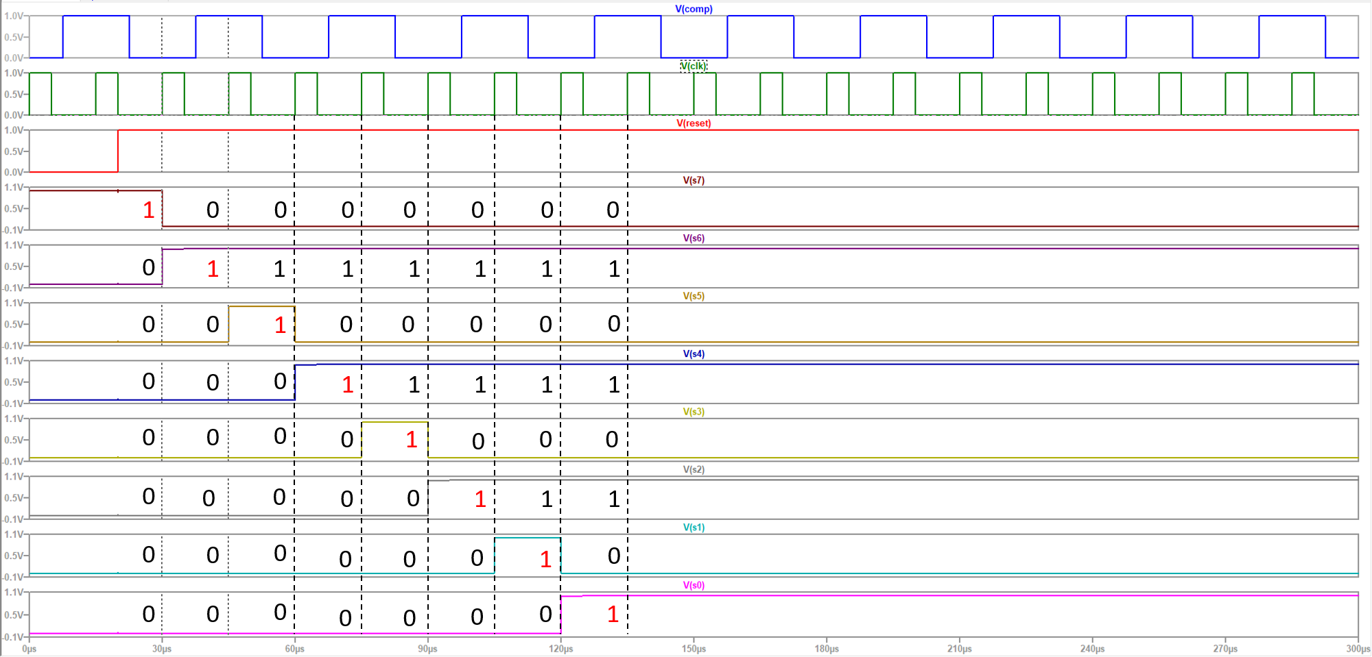
The schematic was ran and produced a cascading structure of 1's in the
waveform for outputs S7-S0, proving that the schematic was correctly
designed. These results can be seen in Figure 10 with each comparator
value displayed alongside an dashed indicator line for the rising-edge
triggered clock.
Figure 10. 8-bit SAR ADC waveform results
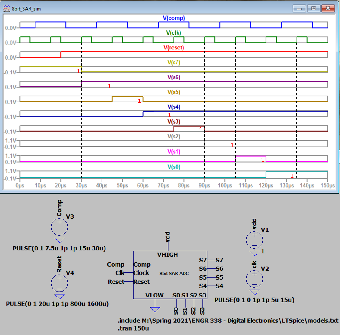
To finish the 8-bit SAR block project off, a symbol was created out of
the schematic for ease-of-use in the future. This was then simulated to
make sure everything was correctly implemented into the symbol. The
waveform and schematic with the new symbol can be seen in Figure 11.
Figure 11. 8-bit SAR ADC Symbol schematic with waveform to prove the correct logic
Discussion
I do
realize that this project was supposed to be larger in scale with the
Sample and Hold, DAC, and other components that make up the entire SAR
ADC. A lot was happening at once this semester and with how the school
handled spring break and external life taking up my energy... I'm very
happy the project was simplified, albeit not the original vision for
our final project. I think this was an interesting project and should
continue to be implemented into future classes as it combines what
we've been learning about throughout the semester and actually seeing
it come to fruition. Simple things like length and width,
structure of the SAR block, and what the waveforms meant, were what
kept me from progressing so once the tutorial was made I knew what I
was supposed to be looking for. With that, I'm glad we were able to
still get the SAR block done and wish the future students who take on
this project good luck.