ENGR338 Lab 2021
Spring
Lab 9 Design a Simple 8-Bit ALU
Name: Sean
Eaton
Email:
smeaton@fortlewis.edu
Design a Simple 8-bit ALU
Introduction
In this lab we were tasked with designing an
8-bit arithmetic logic unit (ALU). The simple 8-bit ALU is able to
perform addition and subtraction arithmetic operations as well as AND
and OR logical operations on two 8-bit inputs. Two selection inputs, S0
and S1, are used to select between the four ALU operations. This lab
built upon previous labs that tasked us with designing 8-bit AND and OR
gates, the 8-bit high-speed full adder, and the 8-bit 2:1 multiplexer.
These schematics, icons, and layouts were used to complete the 8-bit
ALU. The logic of the ALU was simulated previous to the layout view
being created.
Task 1: Design the logic
circuit of the ALU.
The schematic of the ALU was provided to us in the lab instructions and
so it was recreated in Electric VLSI using the appropriate designs that
were created previously in the lab. Only one additional design had to
be created prior to the 8-bit ALU's implementation which was the 8-bit
inverter. The 1-bit inverter design was imported and the process used
in previous labs was used to create an 8-bit inverter. The finished
schematic and icon view are shown below as well as the 8-bit inverter's
layout view.
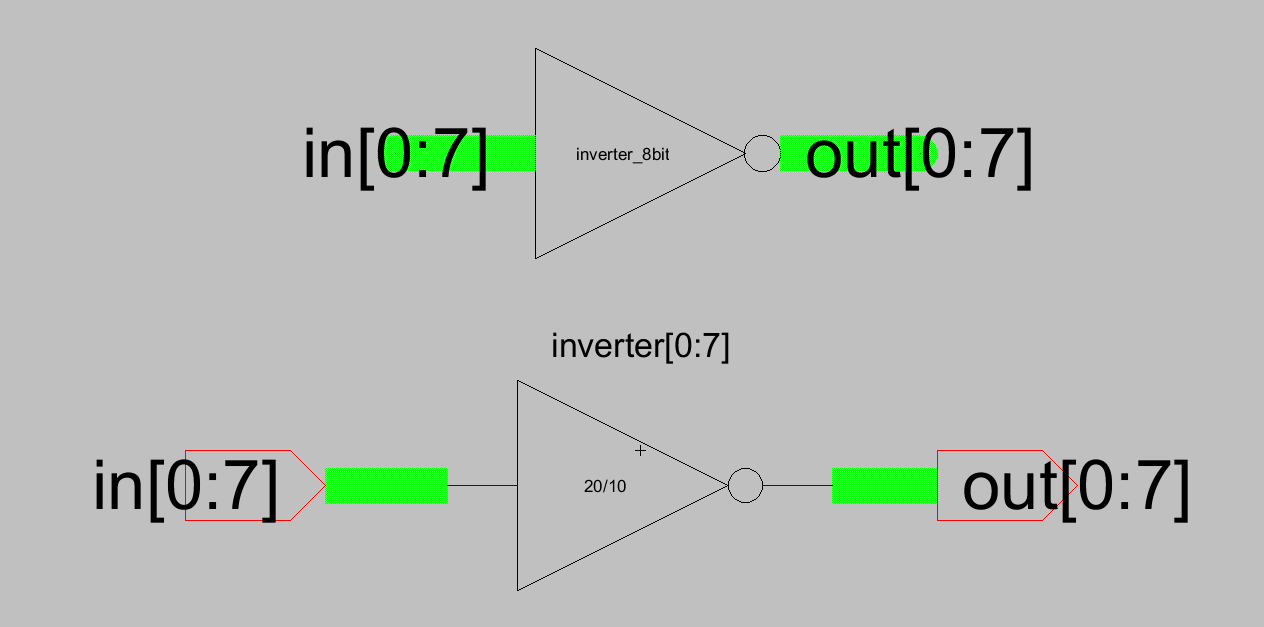
Figure 1. Schematic and icon
of the 8-bit inverter. The icon of the 1-bit schematic was used with
additional bus inputs and outputs.
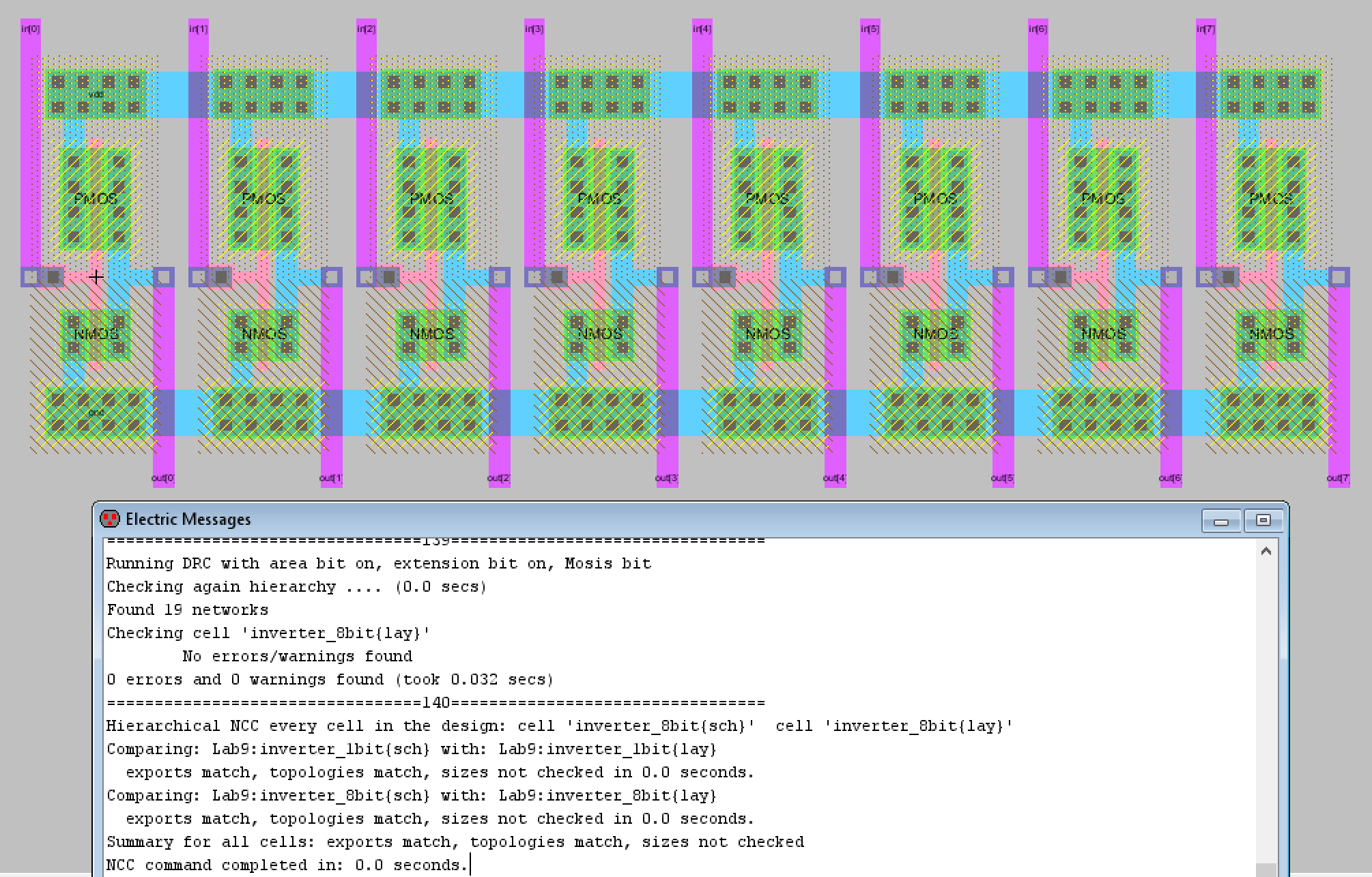
Figure 2. Final layout view
of the 8-bit inverter. The 1-bit inverter's layout view was used to
create the 8-bit inverter's final layout.
Now that an 8-bit inverter was available to use, the schematic of the
ALU was recreated in Electric VLSI. The schematic made use of the 8-bit
AND gate, OR gate, MUX, inverter, and high-speed full adder. Initially
the schematic had the A and B inputs for the 8-bit OR gate reversed but
this was fixed once the layout view was completed. The final schematic
for the ALU is shown below in Figure 3 along with the icon I created.
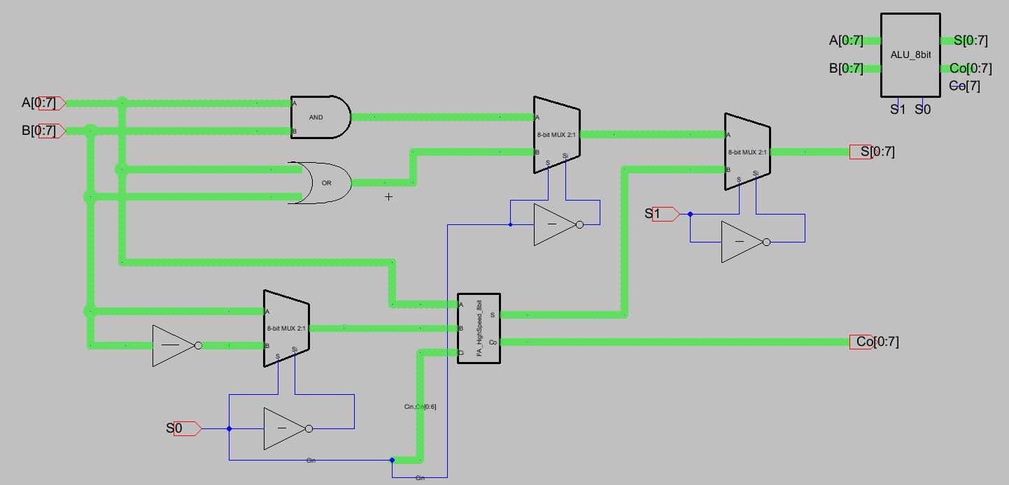
Figure 3. Final schematic
plus the icon for the simple 8-bit ALU.
Now that the schematic and icon were created, it was time to run some
simulations to confirm that the ALU is functioning properly. I decided
to stick with the four examples shown in the lab to verify the ALU's
functionality.
The first simulation verified the AND gate's functionality by setting A
to equal 1111 1111 and setting B to equal 0000 0000. The selection bits
S1 and S0 were set to 00 and the LTSpice simulation performed. Figure 4
below shows the simulation schematic as well as the relevant spice code
used to perform the simulation. Figure 5 shows the LTSpice simulation
waveform plots of the 8-bit S output in addition to the 1-bit Co (carry
out) output. If the ALU was functioning correctly then the expected
output of 0 0000 0000 (Co[7], S[7:0]) should appear which was indeed
verified in the LTSpice simulation.

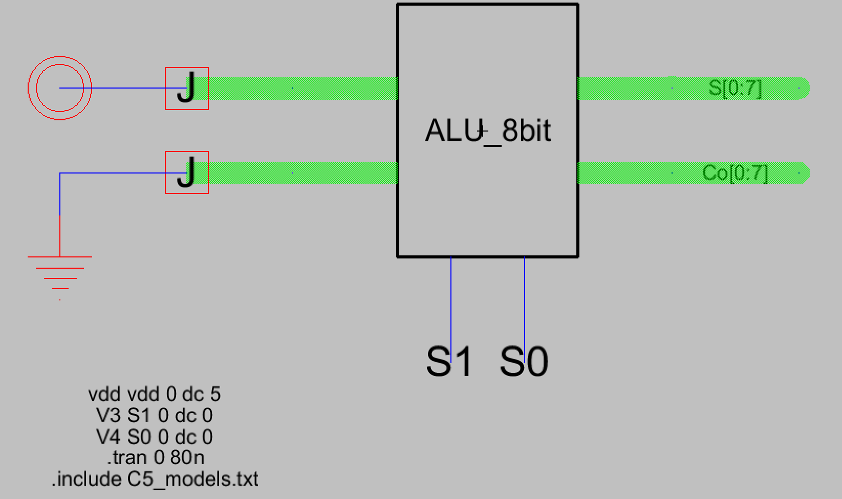
Figure 4. Simulation
schematic for the first simulation performed. A is set to all HIGH
while B is set to all LOW. When an AND operation is performed, the
output should consist of all zeros.
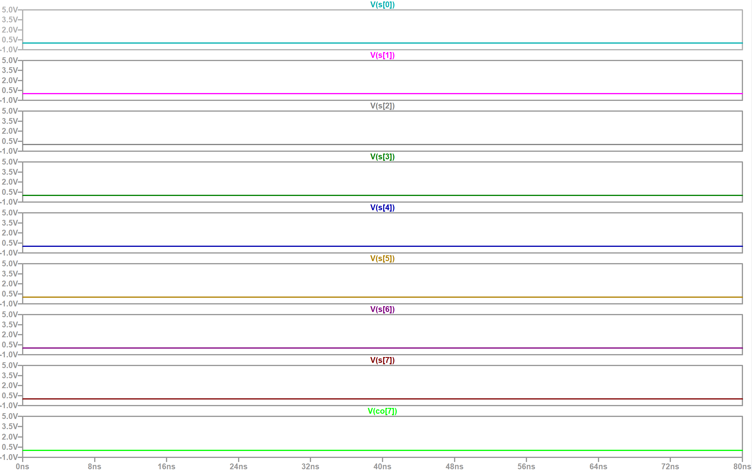
Figure 5. LTSpice simulation
results for the first simulation. The results match the expected
outcome of simulation 1.
The next simulation to be run verified the OR gate's functionality.
This was done by setting the selection bits to 01 while keeping the A
and B inputs the same. Since A consists of all ones and B consists of
all zeros, we expect the output to be all ones or 1 1111 1111 (which is
Co[7] and S[7:0]). This does match the LTSpice simulation results and
so I moved onto the next simulation. Figure 6 shows the LTSpice
simulation results for this test case but I decided not to display the
simulation schematic since there was only a minor change was in the
spice code.
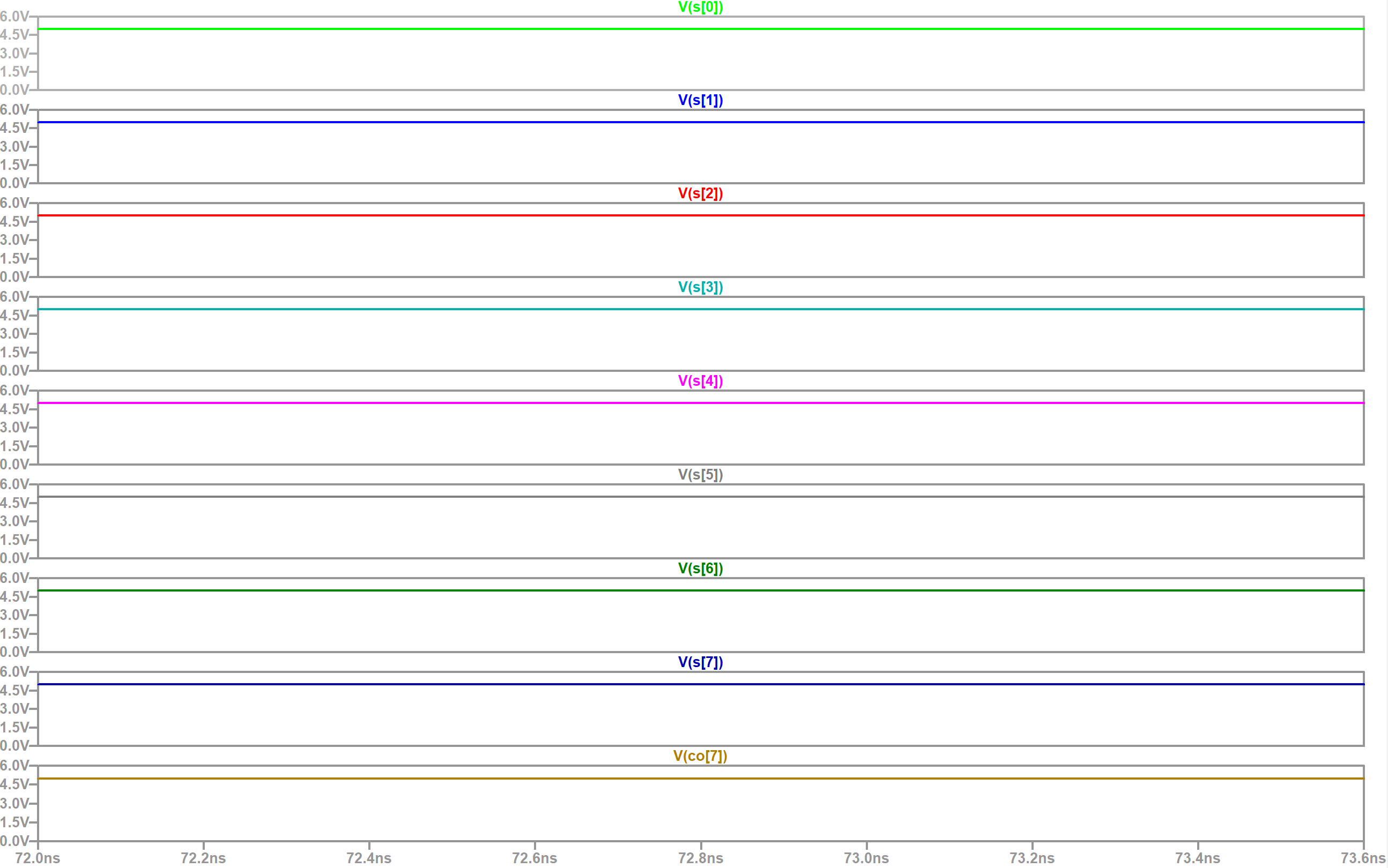
Figure 6. LTSpice simulation
results for the second simulation. The results match the expected
outcome of simulation 2.
The third simulation tested the addition operation. A was set to 1111
1111, B was set to 0000 0001, and the selection bits set to 10. The
expected outcome of this addition was 1 0000 0000 which would be due to
the carry functionality of the ALU operating correctly. The LTSpice
simulation results match this expected outcome and so the addition
operation was verified. Figure 7 displays the simulation schematic for
this simulation since it differed from the previous simulations in
multiple ways. Figure 8 displays the LTSpice simulation results for the
third simulation.
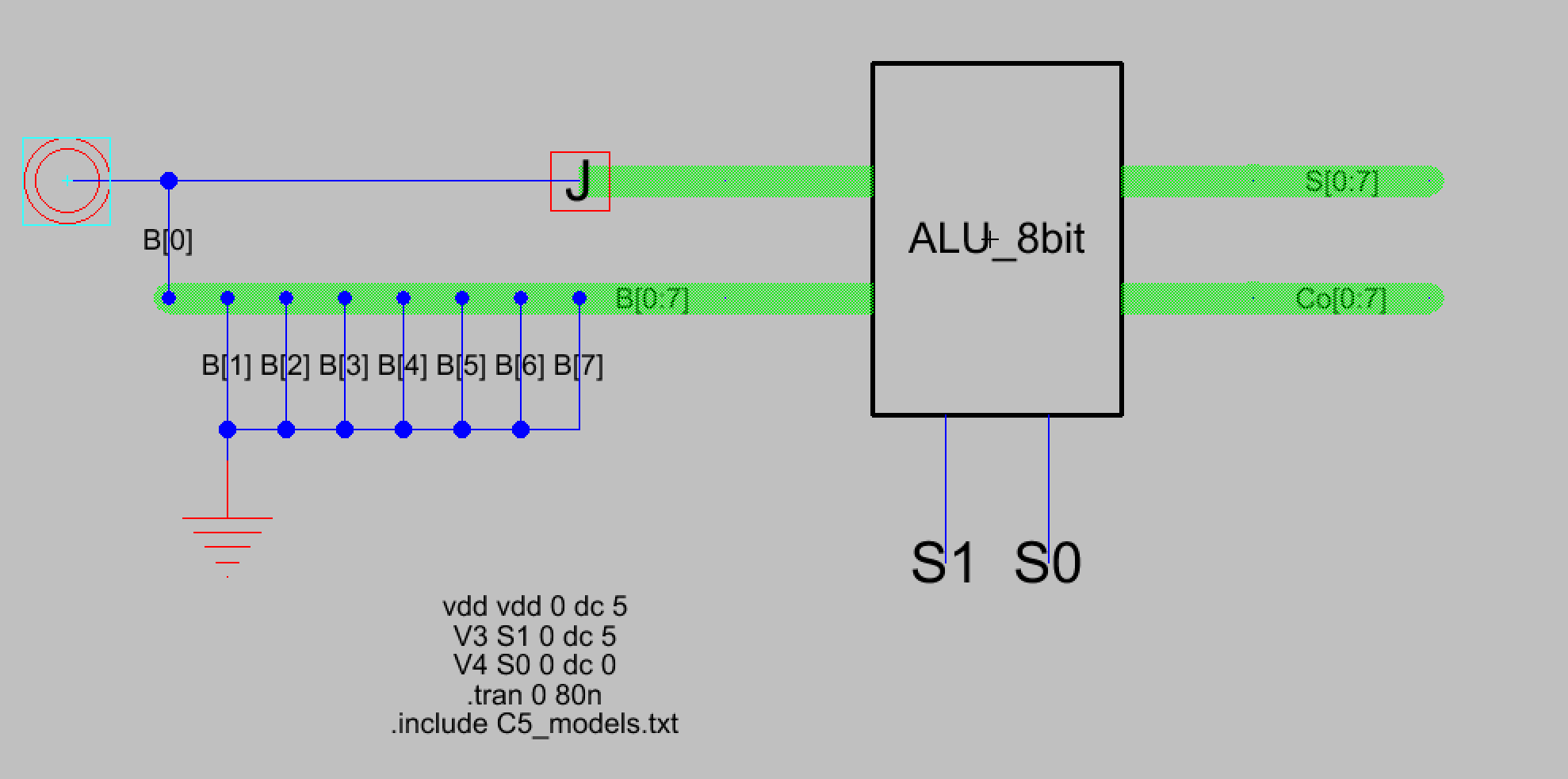
Figure 7. Simulation
schematic for the third simulation, the addition test case.
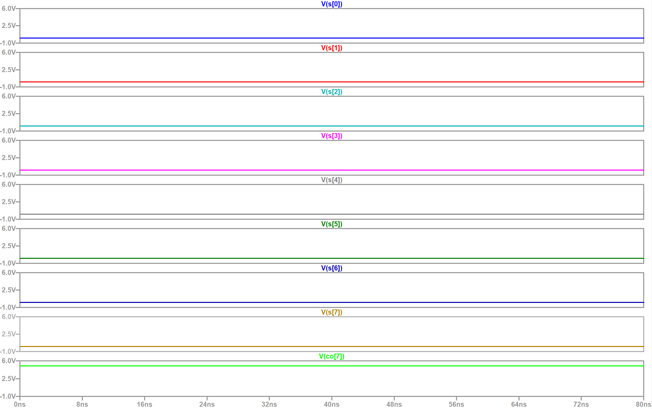
Figure 8. LTSpice simulation
results for the third simulation. The results match the expected
outcome.
The final test case consisted of testing the subtraction operation. The
A and B values were kept the same while the selection inputs, S1 and
S0, were changed to 11. Due to the minor changes the simulation
schematic was omitted. The expected outcome of 1111 1111 - 0000 0001
should be 1 1111 1110 (Co[7] and S[7:0]) due to the 0000 0001
converting to the two's complement version (which is -1). The
functionality was confirm as shown by the LTSpice simulation waveform
shown below.
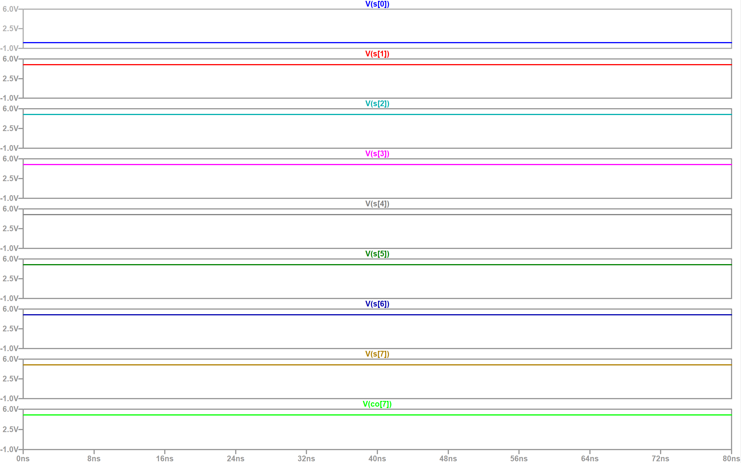
Figure 9. LTSpice simulation
results for the fourth simulation. The results match the expected
outcome of 1 1111 1110.
Now that the functionality of the 8-bit ALU was verified, it was time
to move onto creating the layout view for the ALU.
Task 2: Finish the layout of
the ALU.
For this task we were given a video that gave us tips on wiring a large
scale circuit by hand in addition to some direction given during
lectures. A sample of what the finished ALU layout view could look like
was also provided which was helpful as a starting point. The layout of
the main pieces of the ALU like the AND and OR gates, the MUXes, and
the full adder made sense to me so I tried to lay mine out similarly. I
decided to focus on getting the wiring more compact and thinking about
how to best use the metal layers. My finished layout is shown below in
Figure 10 and you can click on it for a larger view of the layout.
Figure 11 also displays the DRC and NCC check results which were great
to see on the 2nd try.
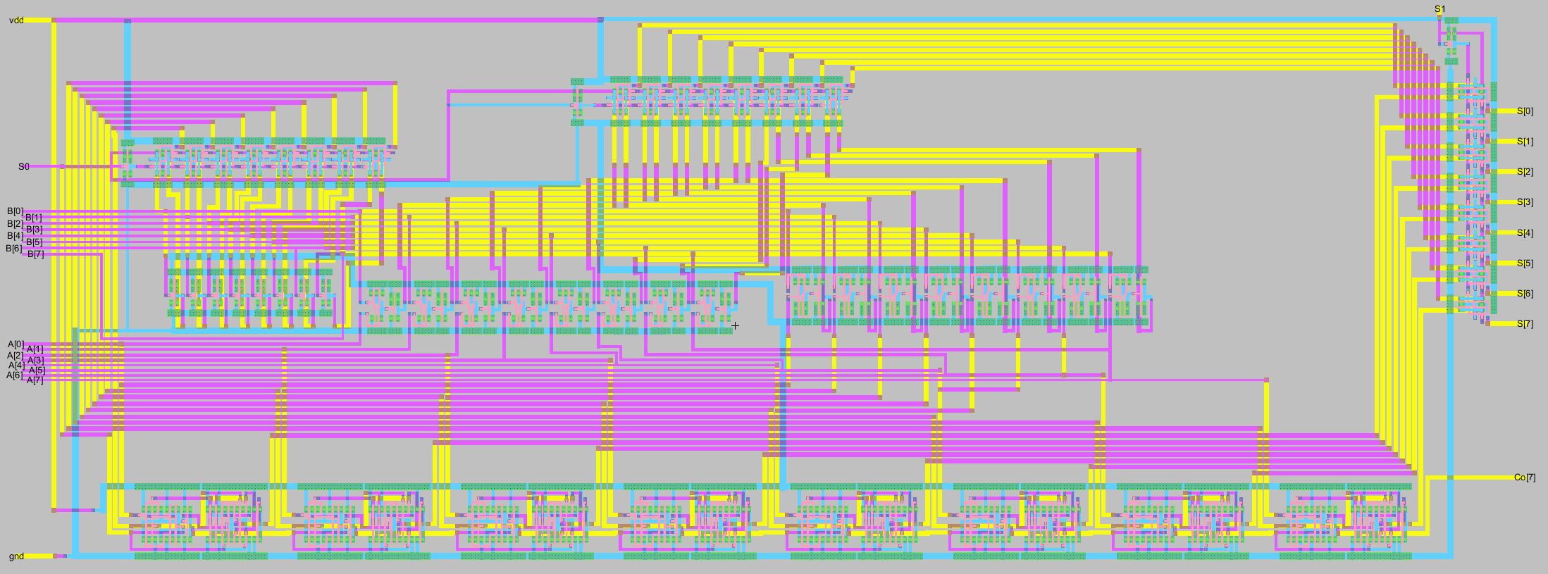
Figure 10. Final layout view
of the simple 8-bit ALU
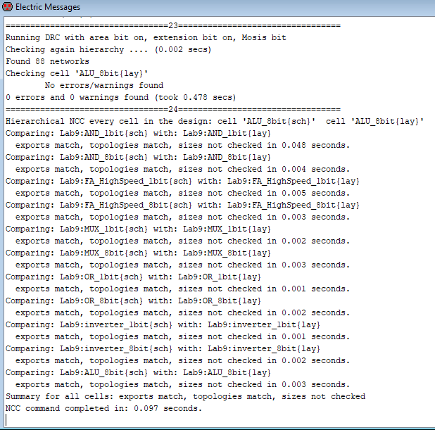
Figure 11. DRC and NCC check
results for the simple 8-bit ALU.
Discussion
I really enjoyed this lab because the design was something that could
actually be useful to have on a PCB. I thought it was really cool to
create a design that had multiple functions rather than the previous
layouts that focused on doing one specific task like the logic gates or
the MUX. It was also awesome to see that the layout design passed NCC
only after two attempts. The first attempt gave me an error on the OR
gate and that was when I realized I reversed the inputs so that B was
going into the A port and vice versa. Thankfully, I was familiar with
the error from a previous lab and I recognized right away that the
simplest fix would be to correct the schematic view to have the inputs
the same as the layout view. I also noticed that it was possible to
only export the Co[7] output instead of the Co[0:7] pins but when I
attempted to do so, I couldn't pass NCC for some reason. I changed the
original export on the schematic to be Co[7] and deleted Co[0:6] on the
layout view, but for whatever reason Electric VLSI wouldn't let the
design pass NCC that way. So I ended up re-adding the exports for all
the carry out outputs. I didn't enlarge the text on those exports
though because they are only used in the full adder and do not have a
pin out. The actual task of laying out the ALU design was a bit
tedious, the worst was starting it because decisions made then would
have to be dealt with later on. Towards the end I decided it'd be
better if I wired the two inputs at the same time so I knew for sure
how the rest of the wires would work, if they followed the correct
pattern.