ENGR338 Lab 2021
Spring
Lab 8 Design a MUX, and a High-Speed Full Adder
Name: Sean
Eaton
Email:
smeaton@fortlewis.edu
Design a MUX, and a High-Speed Full Adder
Introduction
In
this lab we were tasked with designing a 2-1 MUX schematic, icon, and
layout in Electric VLSI. We then had to create an 8-bit MUX using a bus
to create the schematic and eight copies of the 2-1 MUX layout. Next we
were tasked with creating a 1-bit High-Speed Full Adder that used
AND-OR-Inverted (AOI) Logic. The schematic, icon, and layout were then
used for creating the 8-bit High-Speed Full Adder's schematic, icon,
and layout. LTSpice simulations were used to verify the logic for all
the designs. DRC and NCC checks were also performed to verify the
designs.
Task 1: Build an 8-bit MUX
For task one we first were instructed to build the schematic for a 2-1
multiplexer. An image of the schematic for the 2-1 MUX was provided for
us and my final 2-1 MUX schematic and icon are shown below along with
its DRC check results.
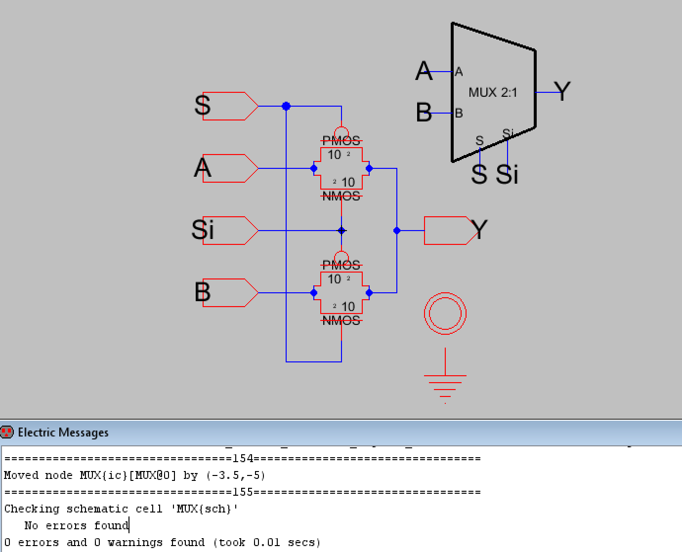
Figure 1. Schematic for the 2-1 MUX with DRC check results.
The logic for the 2-1 MUX was also verified using an LTSpice
simulation. The A, B, S, and Si signals were set to square waves so
that it could be verified in one simulation. The simulation schematic
and LTSpice waveform plot is shown below.
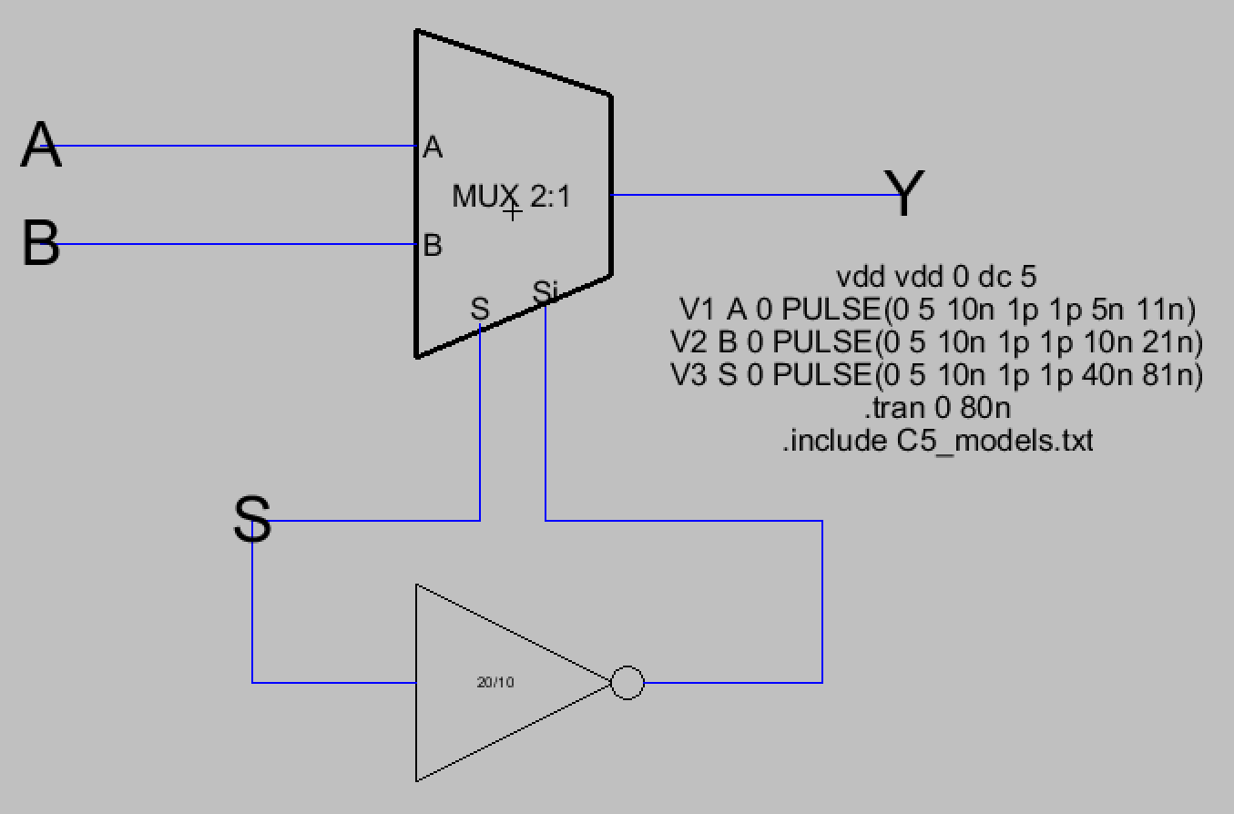
Figure 2. Simulation schematic for the 2-1 MUX along with its spice
code.
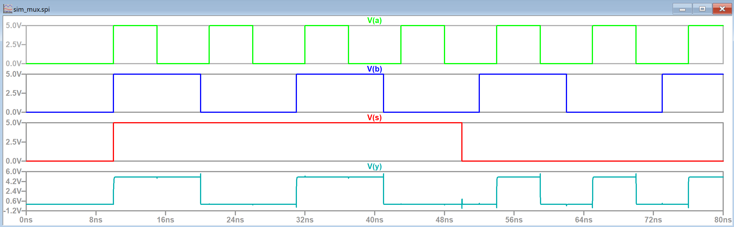
Figure 3. LTSpice simulation waveform results for the 2-1 MUX. V(y)
verified that selection between A and B works correctly.
After this the schematic and icon for the 8-bit MUX was created using
the 2-1 MUX's icon. Buses were used to define that eight 2-1 MUXs in
parallel should be present in the design. An icon for the 8-bit MUX was
also created and the schematic was DRC checked too. The S and Si inputs
used the J wire connection node so that the same S and Si signal
controlled the S and Si inputs for all eight of the MUXes. This way
there wouldn't have to be individual S and Si inputs for each MUX.
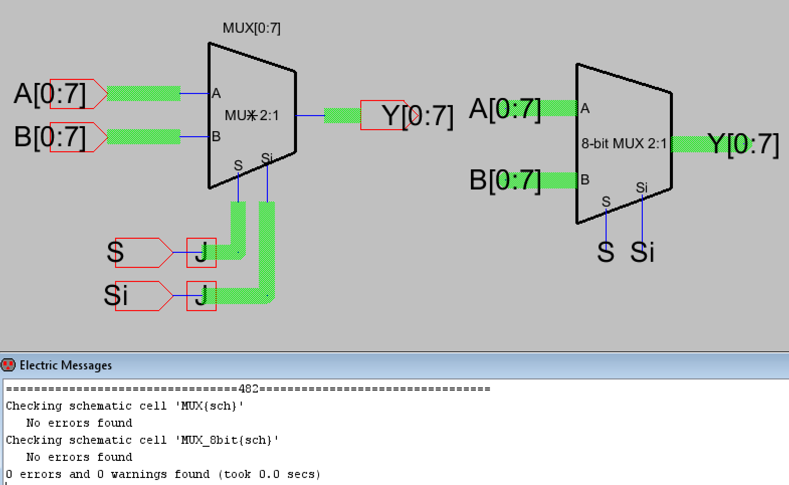
Figure 4. 8-bit MUX schematic and icon along with DRC check results.
The 8-bit MUX also had an LTSpice simulation to verify its
functionality. The simulation schematic and LTSpice waveform plots are
shown below.
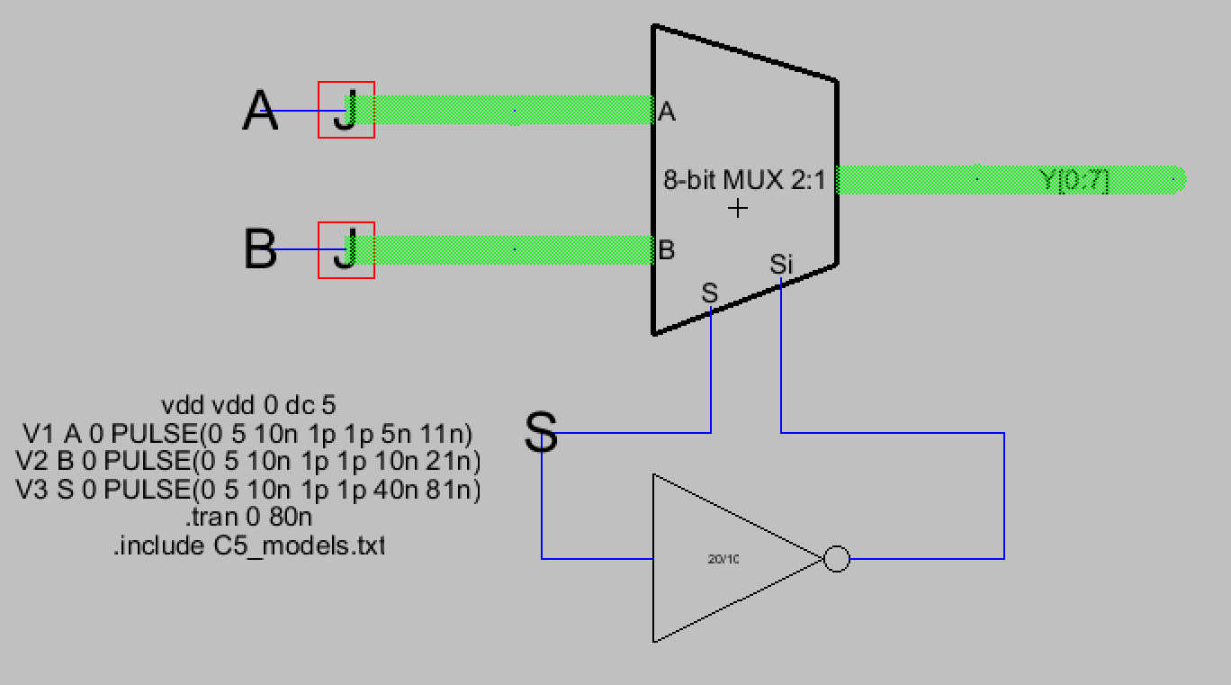
Figure 5. 8-bit MUX simulation schematic with its spice code displayed.
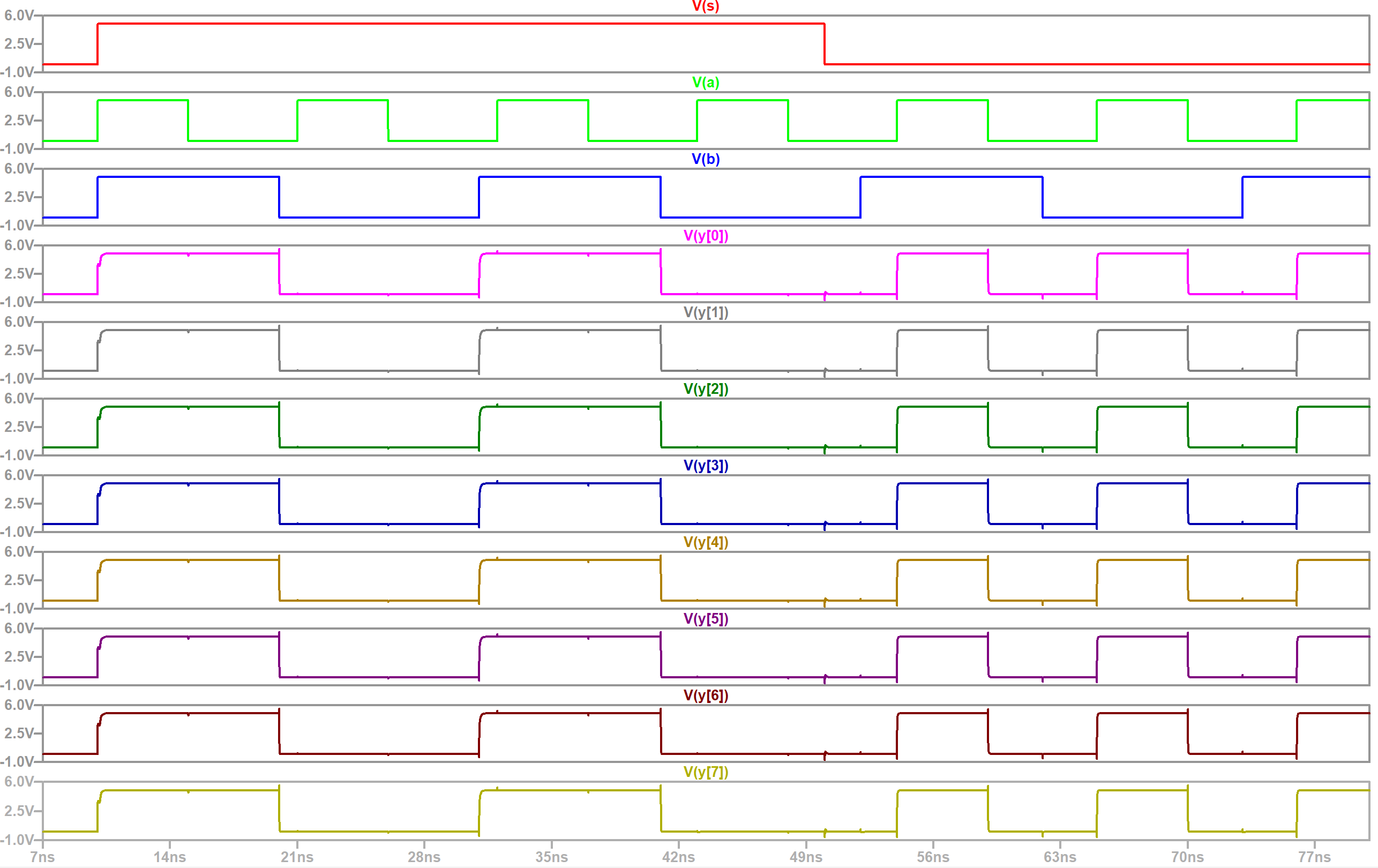
Figure 6. LTSpice simulation waveform plot for the 8-bit MUX. V(y[0:7])
correctly outputs B and then A.
Now that the schematic and icons for the 2-1 MUX and 8-bit MUX were
designed, it was time to create the layouts for them. We started with
the 2-1 MUX since it can be used to create the 8-bit MUX's layout view.
An image of what the final 2-1 MUX layout was provided to us so I
replicated the design, making sure the PMOS and NMOS connections
matched my schematic, and then verified that it passed DRC and NCC
checks.
The 2-1 MUX layout view is shown below in Figure 7. Later on in the lab
it was shown that additional space can be saved by placing the A and B
node on the metal1 arc that connects the pAct and nAct nodes together
so that a metal1 arc doesn't have to protrude as shown below. I added
this fix in when I was creating the layout view and its results can be
seen in Figure 9. A metal1 to metal2 connection node was used in the
same general spot as where the exported A and B nodes used to be.
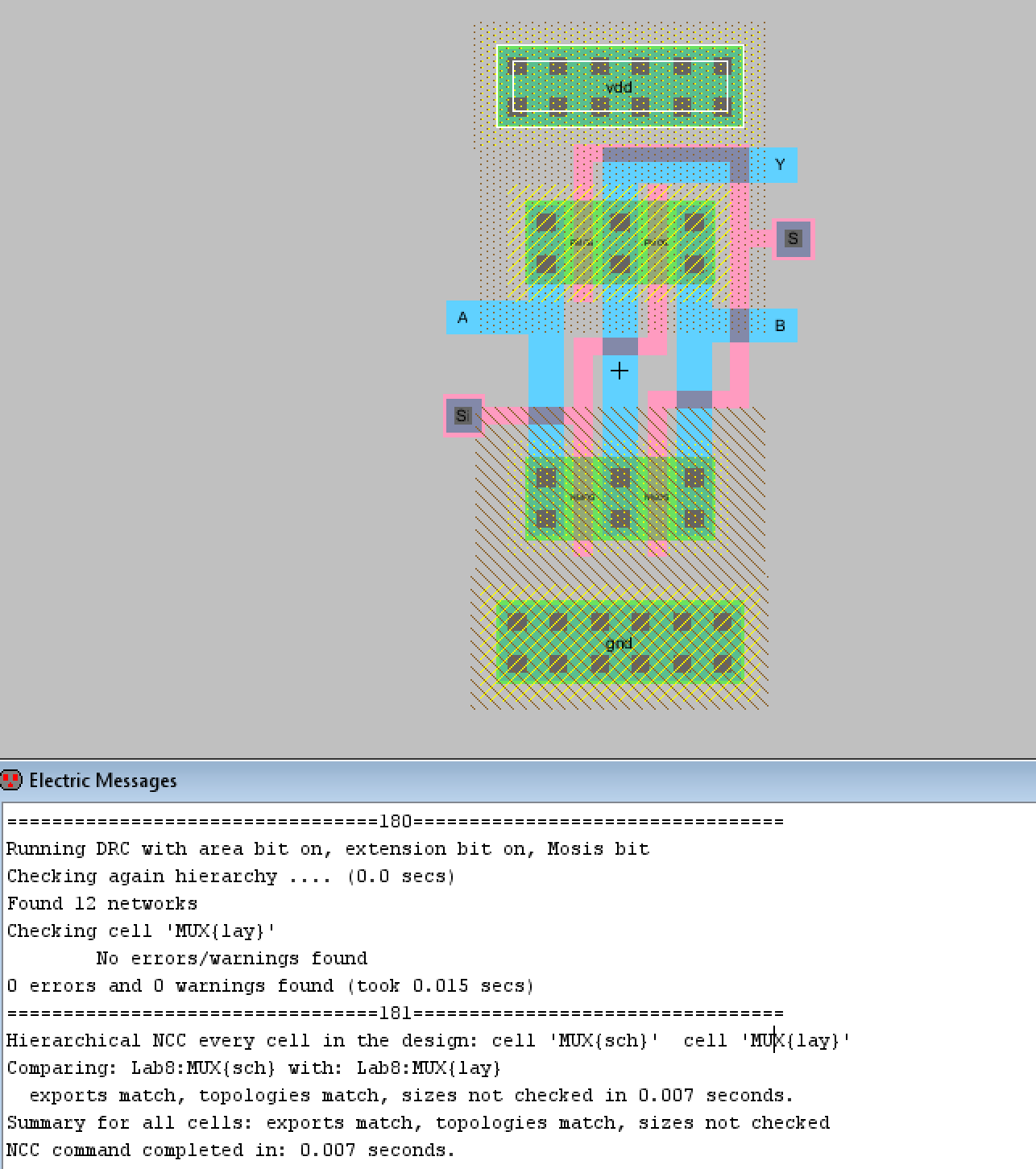
Figure 7. Final layout view for the 2-1 MUX. DRC and NCC check results
are also displayed.
After creating the 2-1 MUX layout view it was then used to create
the
8-bit MUX's layout view. Eight copies of the 2-1 MUX were used to
create the layout. The selection inputs, S and Si, were connected
together so that one single S and Si input was the S and Si inputs for
all eight MUXes. The 8-bit A and B inputs were exported as well as the
8-bit Y outputs, and the VDD and GND inputs. The layout successfully
passed DRC and NCC checks as shown below. A closer view of the 8-bit
MUX layout is shown below as well and the same basic structure was
repeated for all eight MUXes.
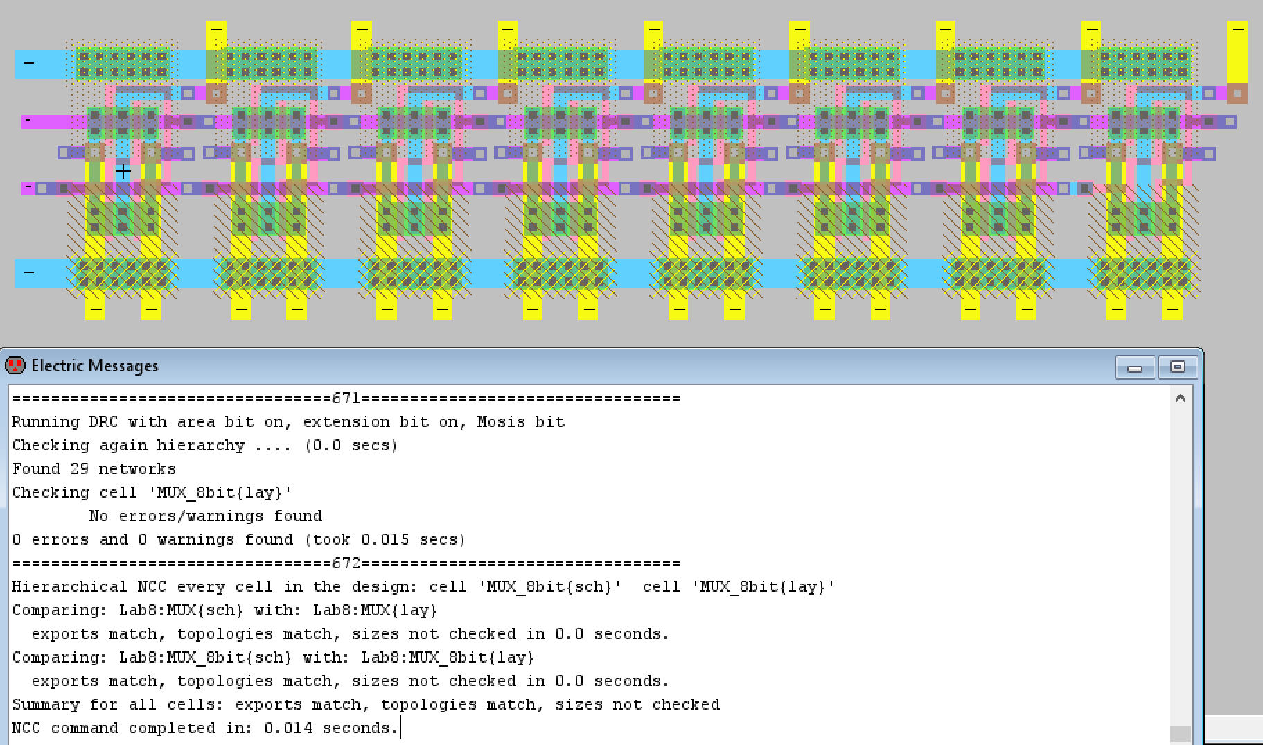
Figure 8. Layout view for the 8-bit MUX with DRC and NCC check results.
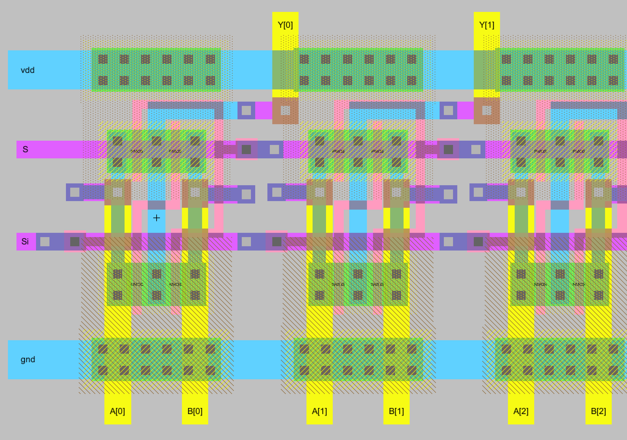
Figure 9. A closer look at what the layout view for the 8-bit MUX looks like.
Task 2: Build a 1-bit high-speed full adder.
Next design to be built was the 1-bit high-speed full adder that uses
AOI logic rather than the logical gate implementation we did in lab 6.
The first thing we did was create the schematic and icon view for the
high-speed full adder. I decided to try to integrate both the summation
portion and the carryout portion together as much as I could so I could
get a better idea of how the layout view connections would work. A DRC
check was also performed before moving on.
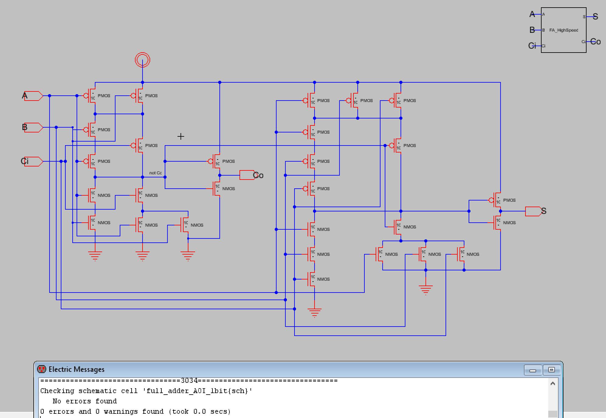
Figure 10. Schematic and icon for the 1-bit high-speed full adder.
Now that the schematic and icon were created, a simulation schematic
was created to verify that the full adder functioned properly. The
simulation schematic and its spice code can be seen below in Figure 11.
Figure 12 shows the LTSpice waveform plot for the A and B inputs along
with the S and Co outputs. Cin was set to high which is why the S
output is set to high for the first 10 nanoseconds or so.
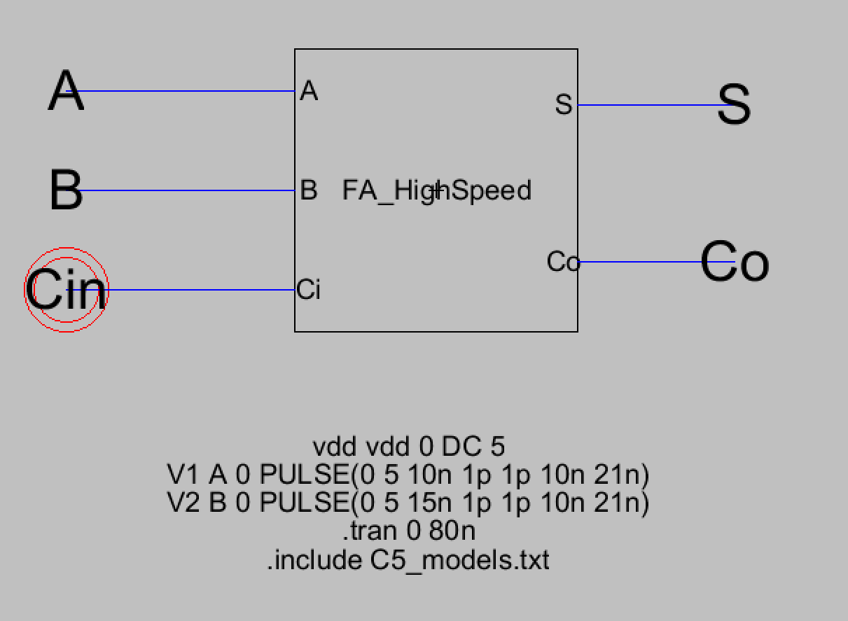
Figure 11. Simulation schematic for the 1-bit high-speed full adder with its spice code.
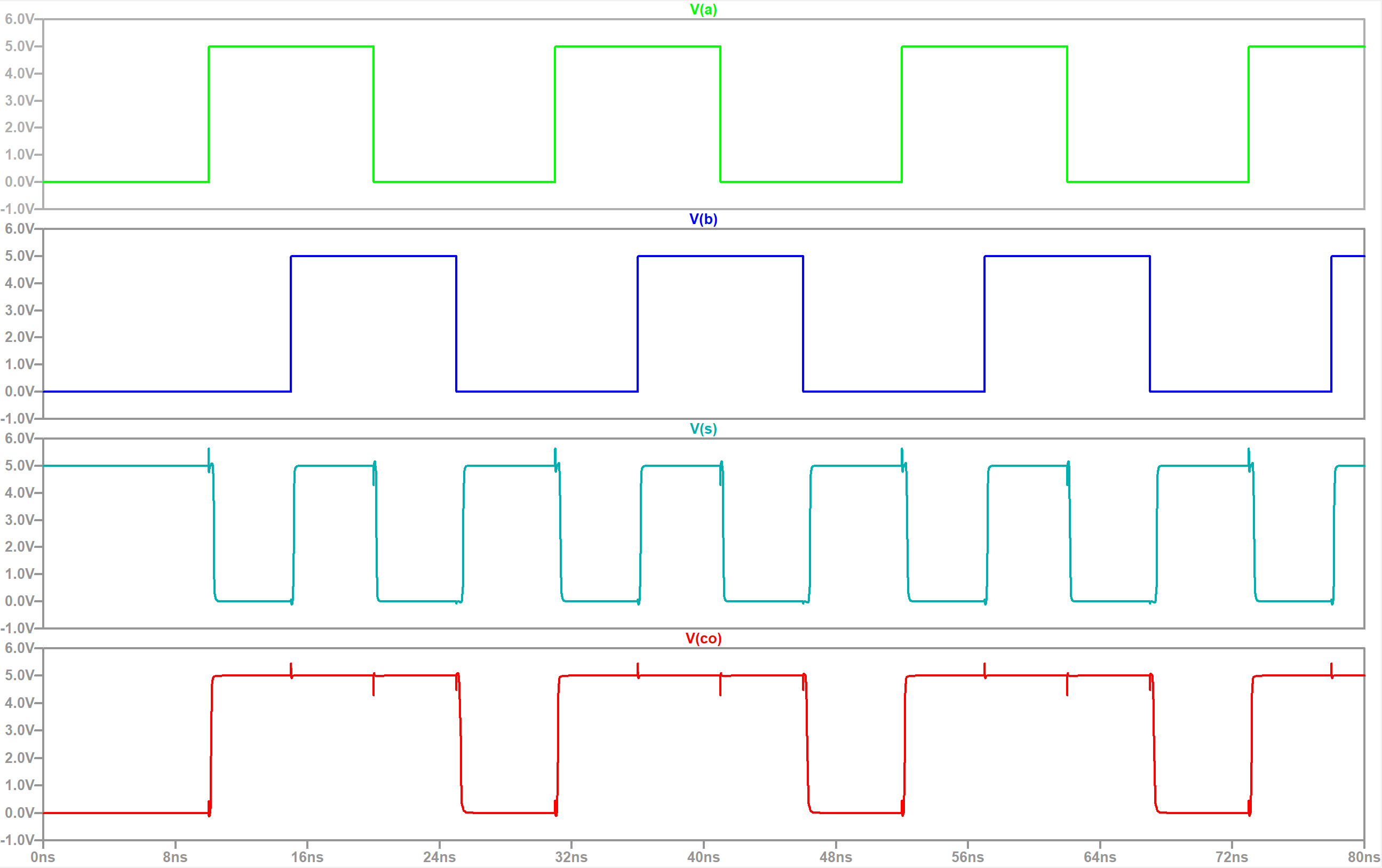
Figure 12. LTSpice simulation waveform plots of the A and B inputs with S and Co outputs.
After verifying the high-speed full adder's logic the layout view had
to be created next. It was advised to use that we should make
connections for each vertical circuit before making the connections
between the vertical parts. I followed this process and then I made the
connections for the gate inputs afterwards while trying to compress the
layout as much as possible with it still passing the DRC check. The
final layout view is shown below along with its DRC and NCC check
results.
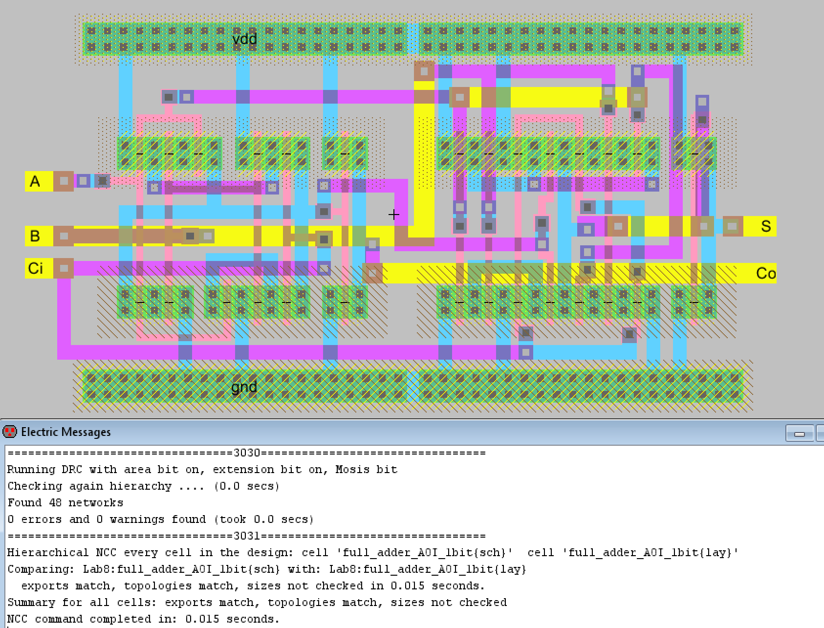
Figure 13. Final layout view for the 1-bit high-speed full adder.
Task 3: Build an 8-bit high-speed full adder.
Now that the 1-bit high-speed full adder was completed we then had to
build the 8-bit high-speed full adder. The schematic and icon were
created first before running simulations to verify the full adder was
functioning properly. The schematic made use of buses and the icon for
the 1-bit high-speed full adder, it also successfully passed the DRC
check as shown below. The A and B inputs were simply 8-bit inputs while
the Carry In (Cin) input was defined as Cin and then Carry Outs 0 to 6
(Co[0:6]). This was because we only actually input Cin as an input. The
rest of the carry outs are passed from one full adder to the next until
we get the final output. The final output will consist of the 8-bit
summation (S) and the 1-bit final carry out C[7].
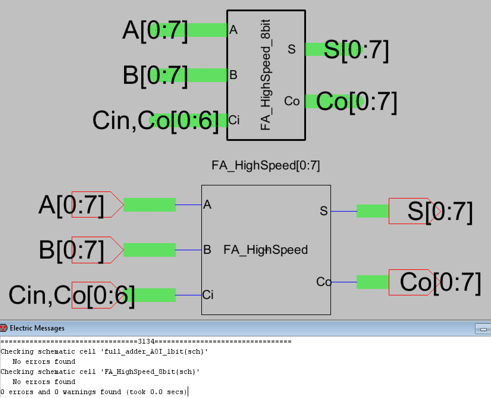
Figure 14. Schematic and icon of the 8-bit high-speed full adder with DRC check results.
After this a simulation schematic was created and three simulations were ran to verify the full adder's functionality.
The first simulation was a replication of the lab's example simulation.
A = 1111 1110, B = 1000 0000, and Cin = 0. The expected result should
be Co = 1, S = 0111 1110 or 1 0111 1110. The LTSpice simulation
waveform plot is shown below and displays the summation output along
with the final carry out.
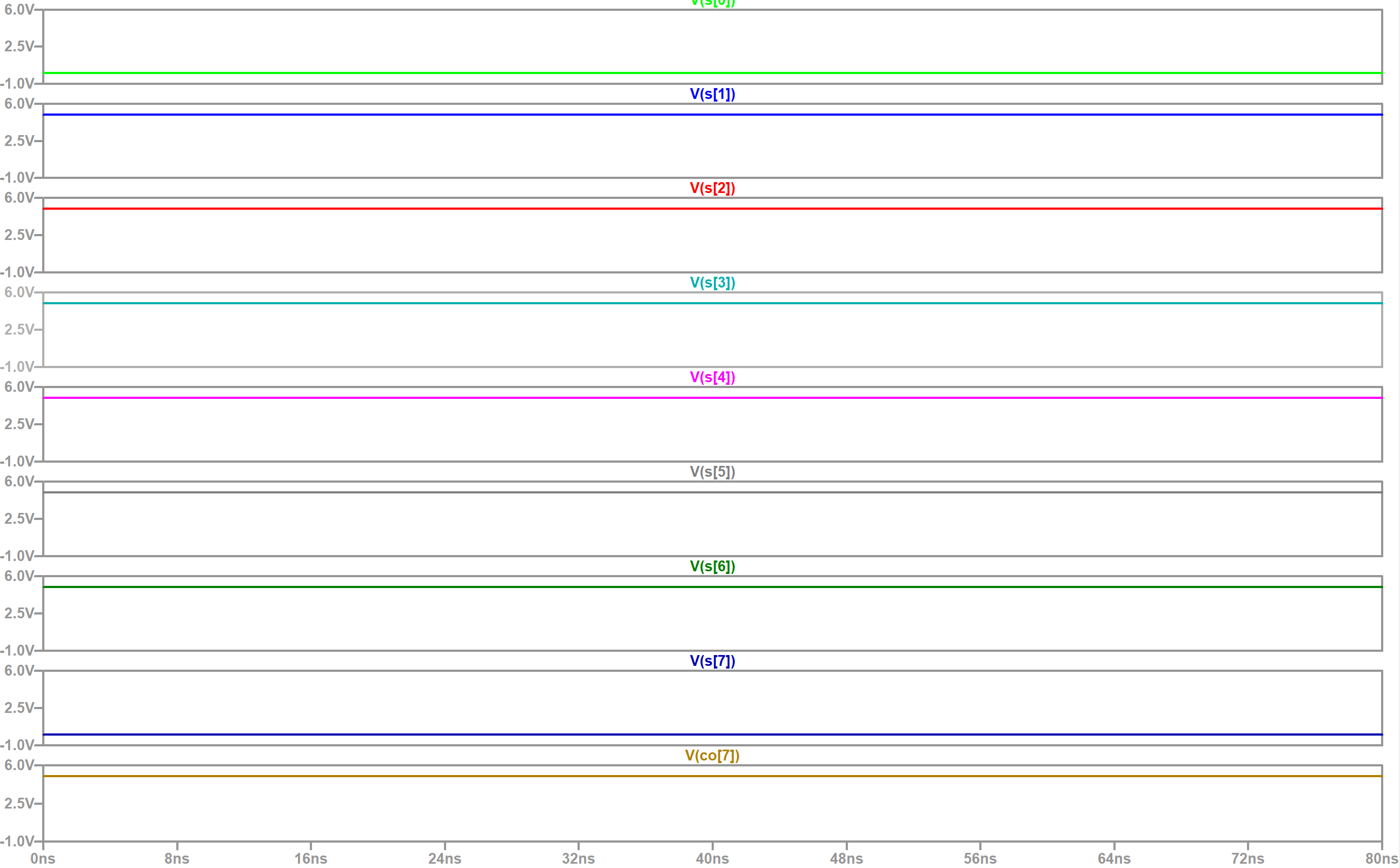
Figure 15. LTSpice simulation waveform results for the first simulation. Result is equal to 1 0111 1110 as expected.
The second simulation had A = 1010 1010, B = 0101 0101, with Cin = 0.
The expected result should be 0 1111 1111 which is what was seen in the
LTSpice waveform plots of S[0:7] and Co[7].
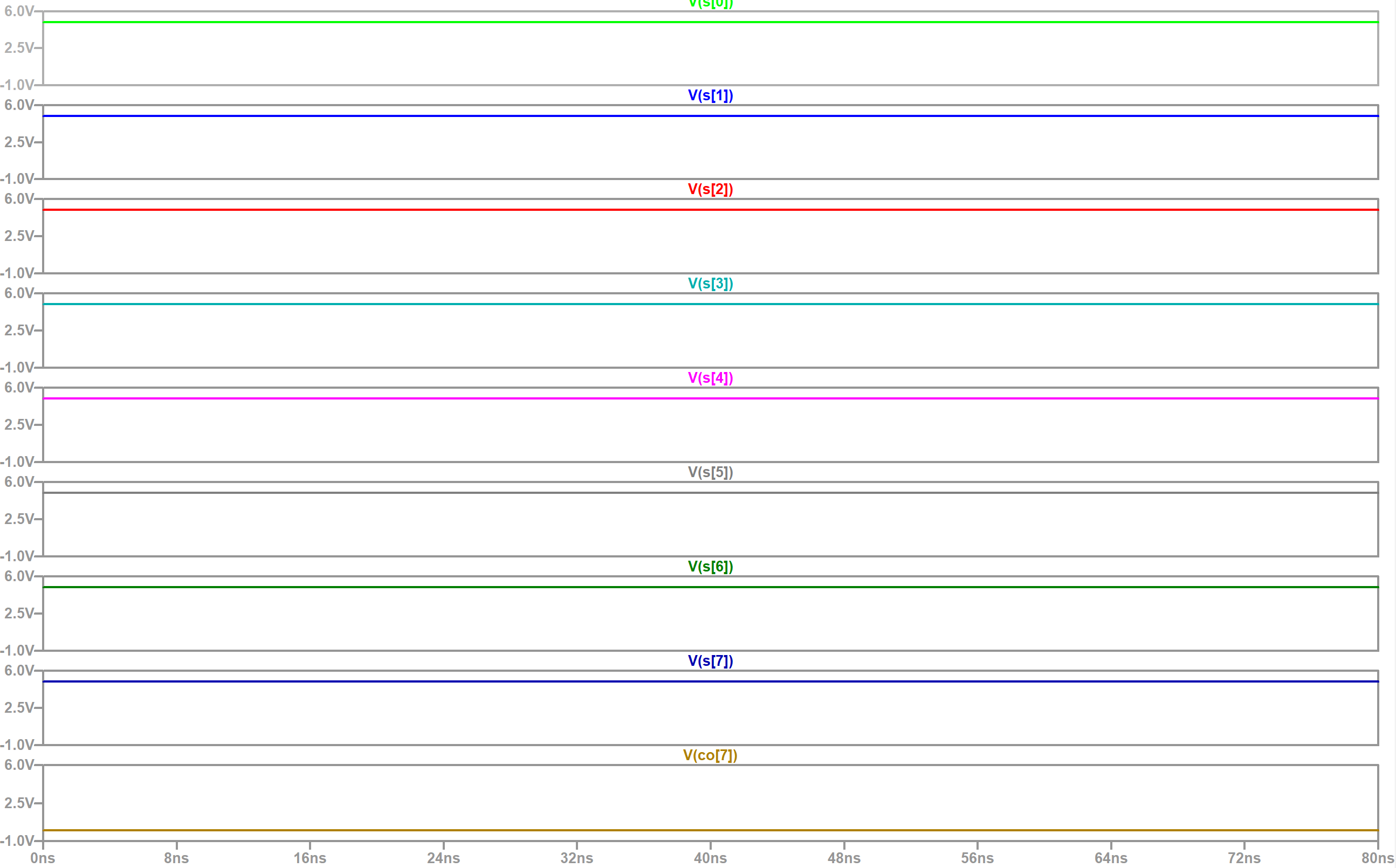
Figure 16. LTSpice simulation waveform results for the second simulation. Result is equal to 0 1111 1111.
The third and final simulation had A = 1001 0110, B = 1101 0010, and
Cin = 1. I designed this one so that the result will be 1 0110 1001
which has S being the digits of A reversed. I also wanted to verify
Carry In functionality since I didn't set Cin to 1 in the previous two
simulations. The results are shown below in Figure 17.
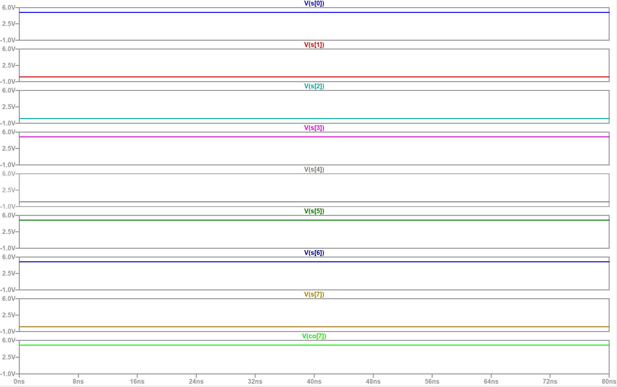
Figure 17. LTSpice simulation waveform results for the third simulation. Result is equal to 1 0110 1001.
The simulation schematic used for the final simulation is shown below
in Figure 18. The first two simulations used a modified version of this
schematic to change the A, B, and Cin inputs so I decided to just show
the final one since it verified Carry In functionality. A, B, and Cin
inputs were changed by connecting the individual wires' connections to
either VDD or GND.
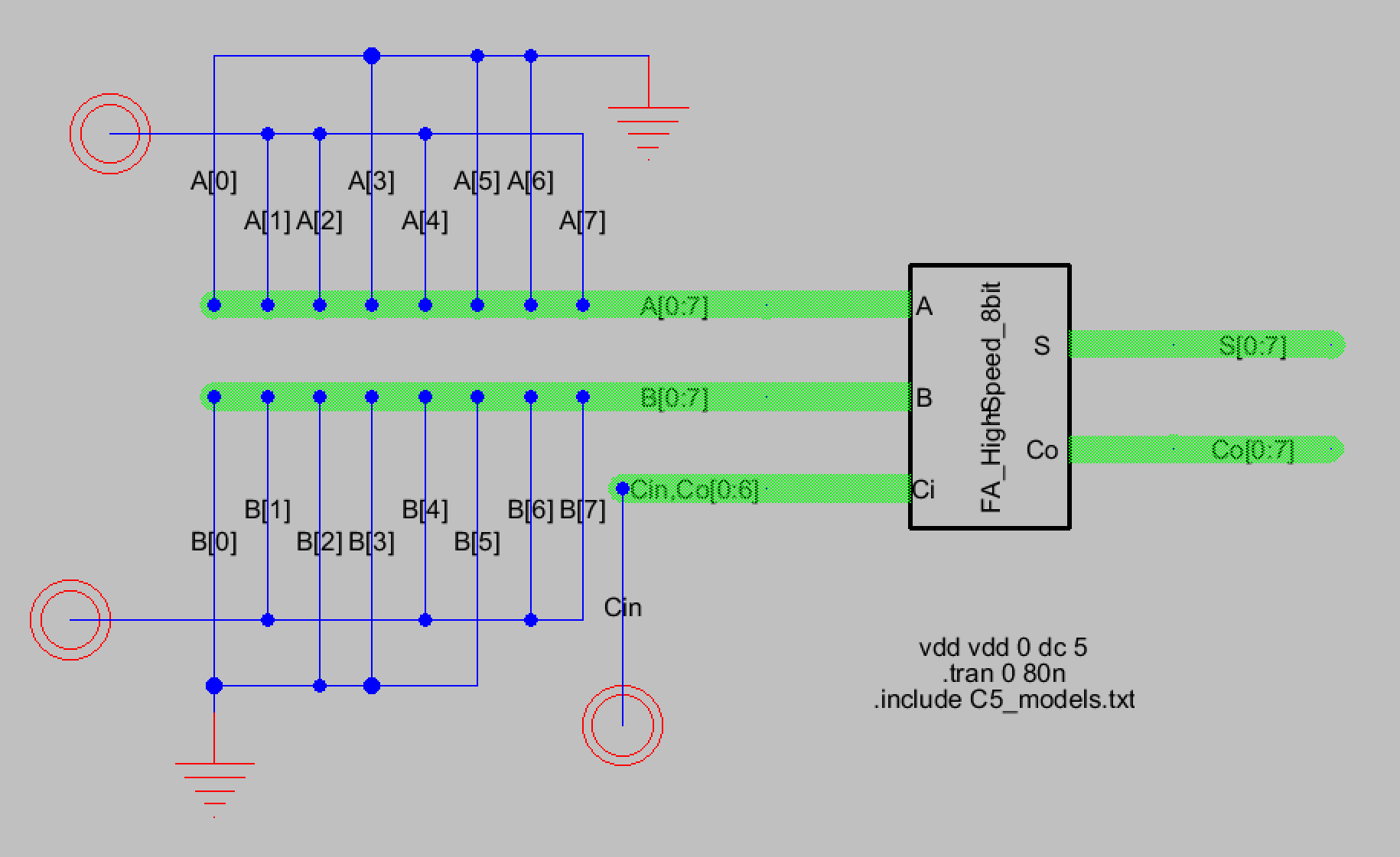
Figure 18. Simulation schematic for the third simulation. A = 1001 0110, B = 1101 0010, Cin = 1.
Now that the logic for the 8-bit MUX had been verified it was time to
create the layout view for it. Eight copies of the 1-bit high-speed
full adder were used to create the 8-bit high-speed full adder. Exports
were made for the 8-bit A and B inputs, the 1-bit Cin input, the 8-bit
S output, and the 1-bit final carry out, Co[7]. In between each full
adder the previous full adder's carry out was connected to the next
full adder's carry in. These connections also had to have a pin
exported as a Co output from Co[0] up to Co[6] so that the layout would
pass the NCC check. The final 8-bit full adder layout with its DRC and
NCC check results is shown below in Figure 19. A closer look at the
8-bit full adder is also shown in Figure 20.
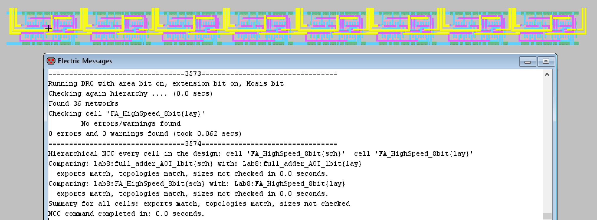
Figure 19. Final layout view of the 8-bit full adder along with good DRC and NCC check results.
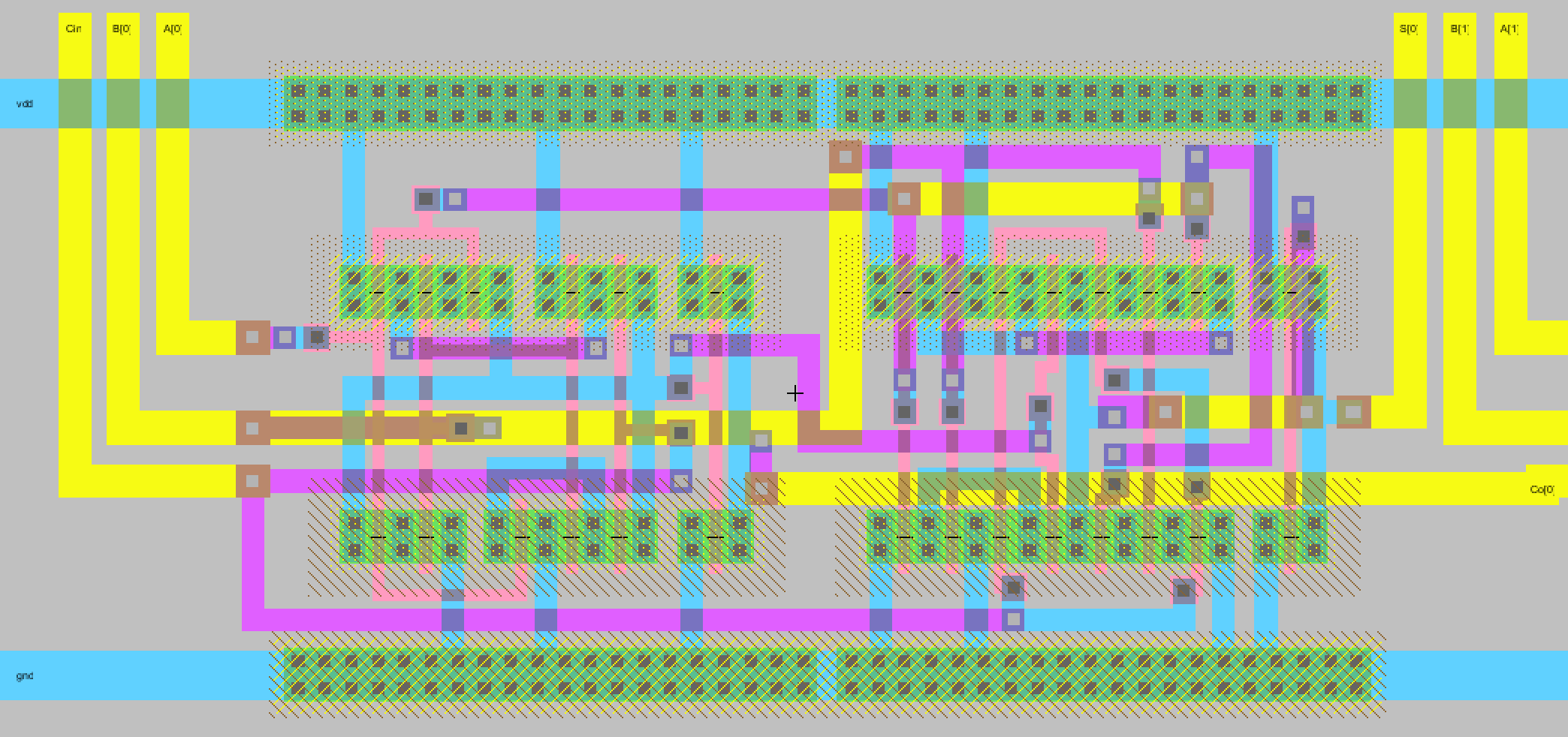
Figure 20. A closer look at
the 8-bit high-speed full adder layout. Co[0] on the right connects to
the next full adder's Cin input.
Discussion
This lab was more
challenging for me than previous labs due to having to design the 1-bit
high-speed full adder's layout. The general outline of the layout
wasn't difficult but connecting each transistor to its required input
was challenging. The A, B, and Cin inputs had to travel pretty far and
I had to really think about how to best use the metal1, metal2, metal3,
and poly arcs so that the layout remained as small as possible. In
addition to this the inverse carry out output also had to connect to
transistors. I also had to switch my A and B inputs for the two PMOSes
on the left below the first PMOS with an A input on top. Previously it
was A, then B, but I had issues with my layout when I did the NCC
check. After debugging there ended up being a part mismatch with the
first two PMOSes so rather than edit the layout (which caused more
errors) I decided to change the schematic instead. I verified
functionality with the simulation before calling it complete. I am
happy with how my layout came out and I'm sure I could improve on it
more since I'm more familiar with the neccessary connections.
I didn't have any issues with the 2-1 MUX and 8-bit MUX although I
wanted to modify the MUX design to be like the MUX I created for HW3.
The HW3 MUX I created included an additional PMOS and NMOS for
inverting the selection input, eliminating the need for both S and Si
inputs. I decided however to just stick with what the lab required. The
final 8-bit high-speed full adder also didn't cause me any troubles,
the process isn't that difficult once the initial layout view has been
created. I enjoyed having to figure out the best way to layout the
1-bit high-speed full adder.