ENGR338 Lab 2021
Spring
Lab 6 Build a NAND, NOR, XOR, and Full Adder
Name: Sean
Eaton
Email:
smeaton@fortlewis.edu
Build a NAND, NOR, XOR, and Full Adder
Introduction:
In this lab we were tasked with creating schematics, icons, and layouts
for a NAND, NOR, and XOR gate. We then used these gates to create the
schematic, icon, and layout of a full adder. All of these gates and the
full adder were created using AND-OR-Invert (AOI) Logic with PMOS and
NMOS transistors.
Task 1: Create the schematic and layout of the NAND gate.
The first gate to be built was the NAND gate. I added the appropriate
PMOS, NMOS, VDD, and GND symbols to the schematic, exported the inputs
and outputs, and created the icon view to resemble what the NAND gate
symbol looks like. The schematic, icon, and DRC check results are shown
in Figure 1 below. The PMOS and NMOS transistors had a width of 10 and
a length of 2 and had their spice models set appropriately. I also
followed the instructions in order to get the NAND gate shape right by
editing the circle properties.
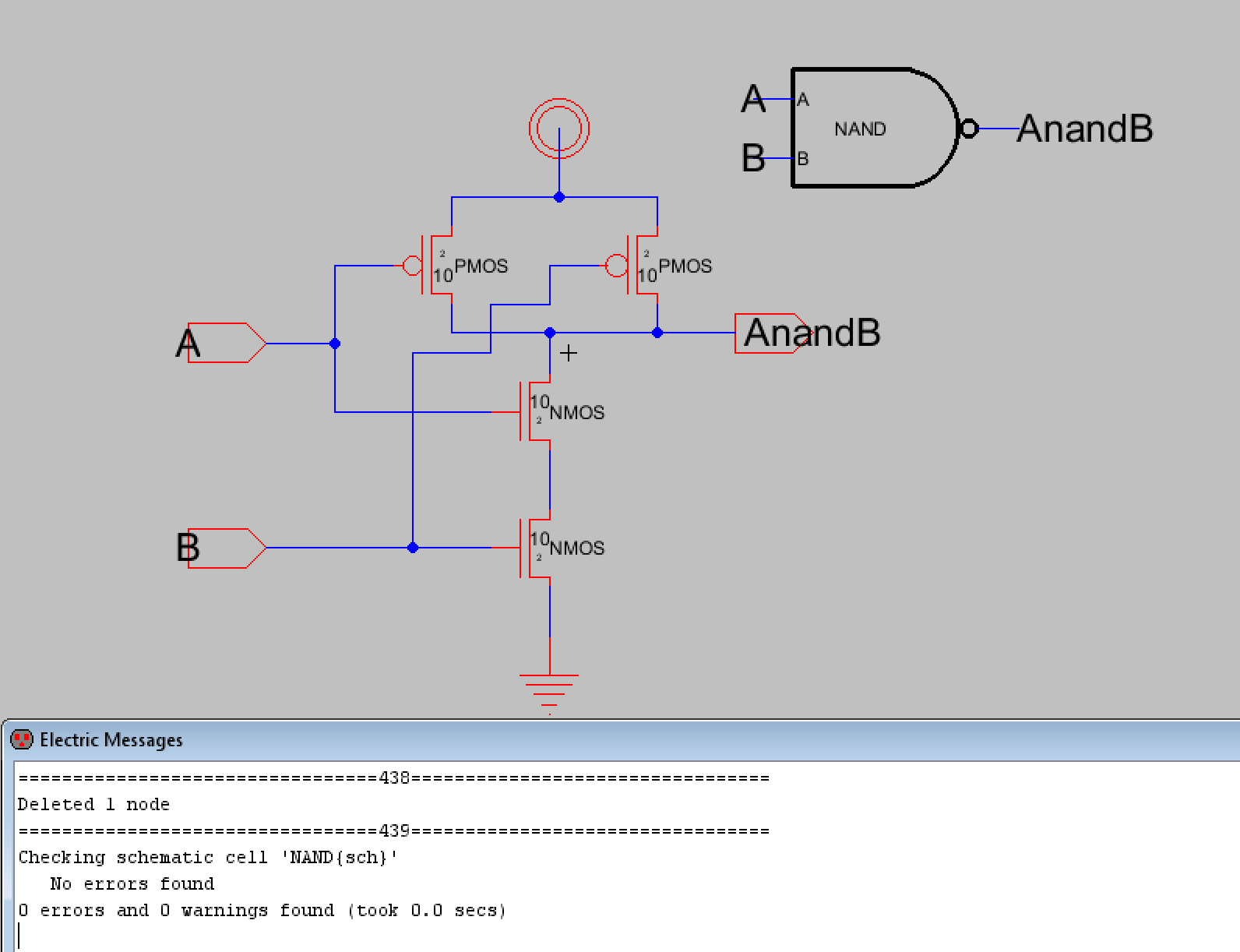
Figure 1. Schematic view of
the NAND gate. The icon can be seen in the upper right corner. DRC
check results are shown at the bottom.
Next a simulation schematic was created that used the icon of the NAND
gate along with spice code to verify NAND gate logic. This is shown
below in Figure 2. Figure 3 shows the LTSpice simulation waveform
results for the NAND gate. Since VDD is always set to high, V(out) is
only high when V(in) is low.
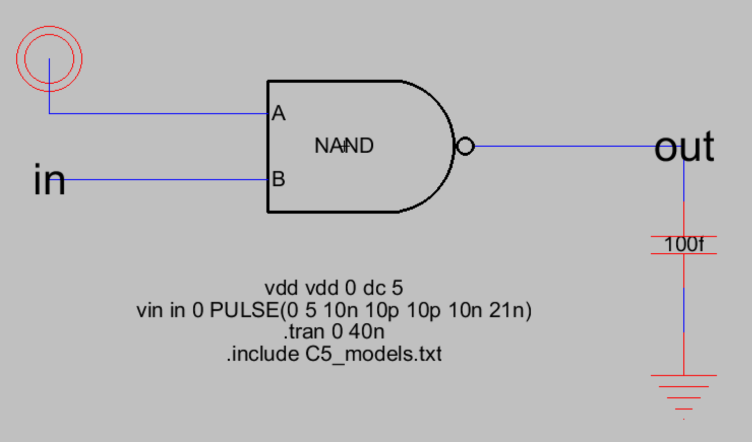
Figure 2. Simulation schematic for the NAND gate.
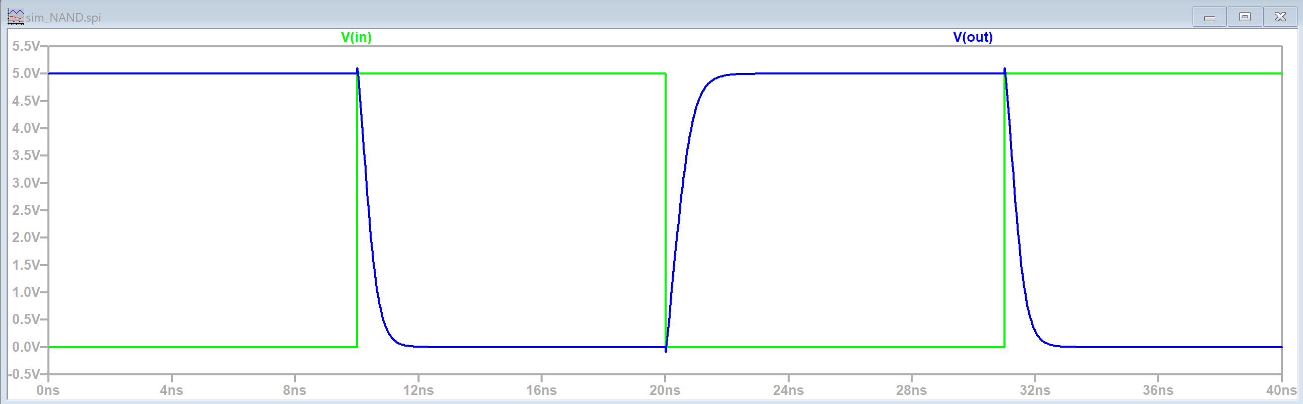
Figure 3. LTSpice simulation waveform results for the NAND gate.
Now that the schematic was free of DRC errors and the NAND gate logic
was verified, it was time to work on the layout view. I first added the
required PMOS, NMOS, nAct, and pAct nodes and arranged them according
to the lab instructions. Figure 4 shows these nodes with the necessary
connections.
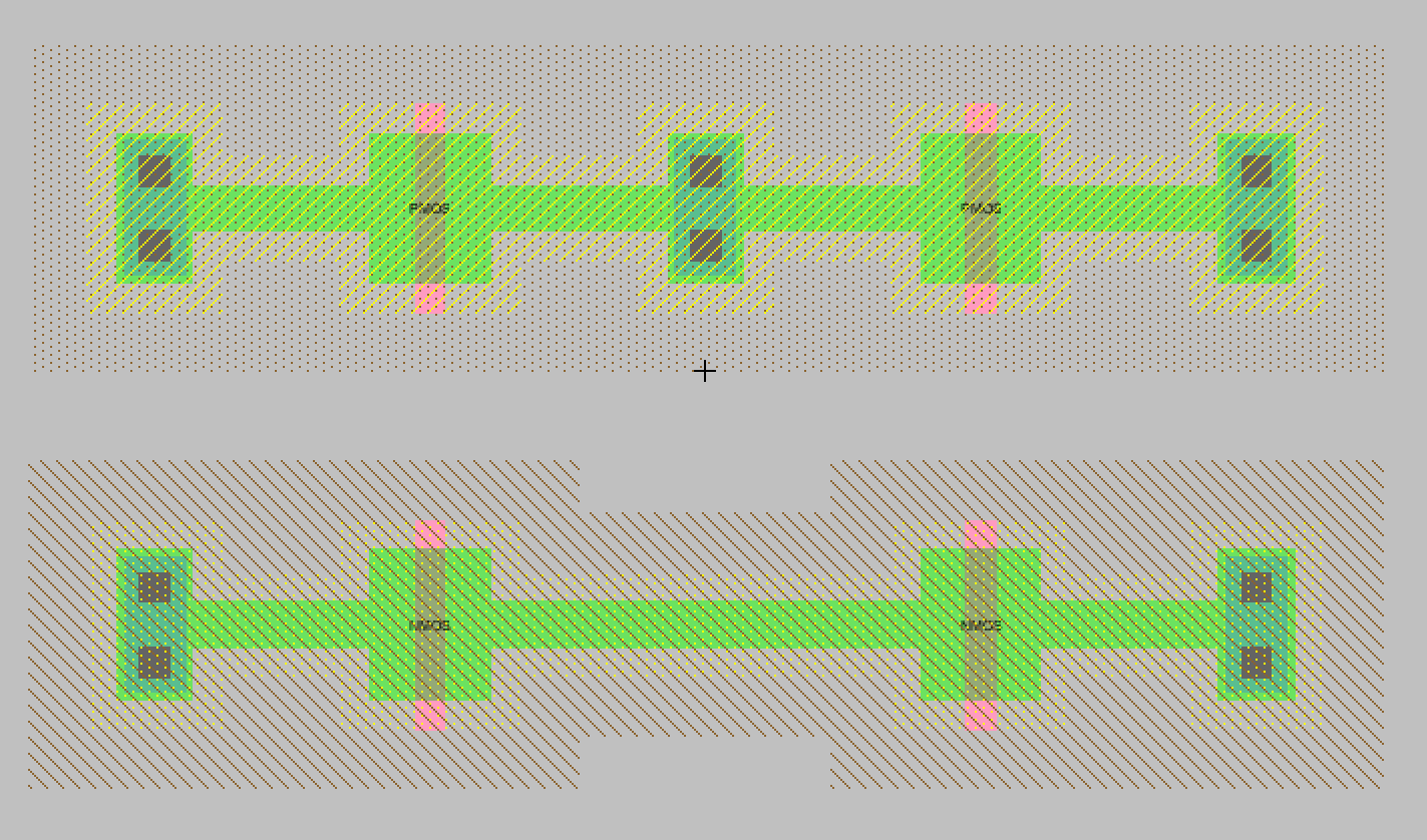
Figure 4. Initial layout view with the PMOS, NMOS, nAct, and pAct nodes connected together.
I then moved them closer together making sure that the distances passed the DRC check. The results are shown in Figure 5.
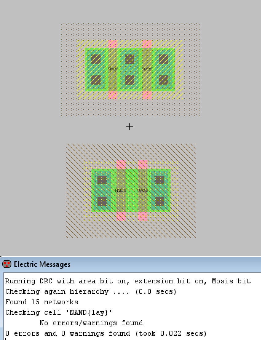
Figure 5. Nodes have been positioned closer and DRC check passes.
At this point I hadn't added the pWell or nWell nodes yet so I added
them, adjusted their x and y sizes to match the lab's example of what
the layout should look like, and then I made the necessary connections
and exported the appropriate pins. The final layout view is shown in
Figure 6 below. Figure 7 also displays the DRC check and NCC check
results (which were good).
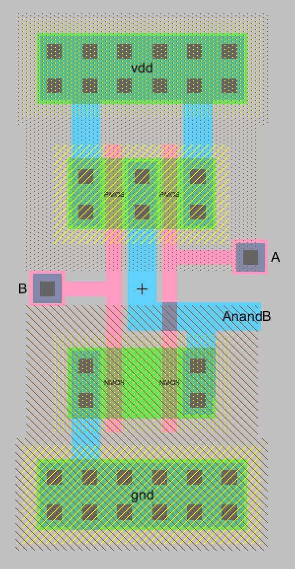
Figure 6. The final layout view for the NAND gate. All necessary connections have been made and pins exported.
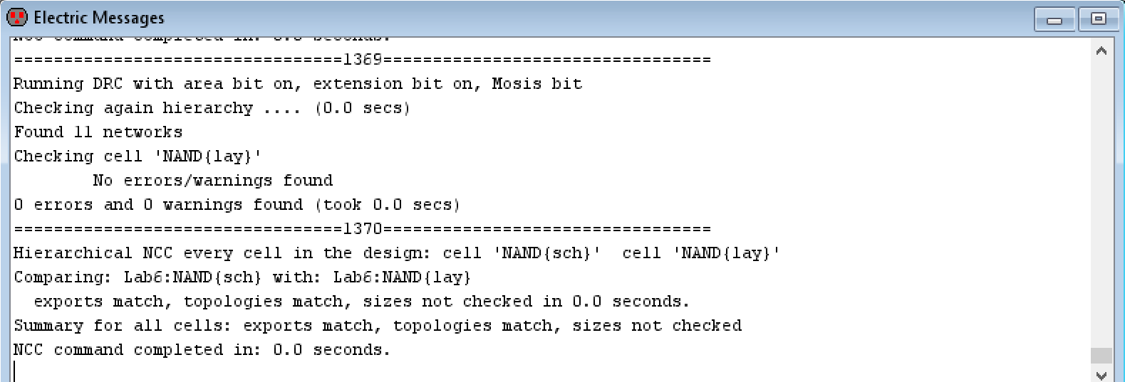
Figure 7. DRC and NCC check results for the layout view of the NAND gate.
Task 2: Create the schematic and layout of the NOR gate.
The next gate to be created was the NOR gate. The process of building
the NOR gate was similar to building the NAND gate. First the schematic
and icon views were created which can be seen in Figure 8. Figure 8
also shows the DRC check results for the schematic view. Lab
instructions were followed for created the NOR gate symbol. Also, for
the NOR gate the width of the PMOS transistors was specified to be 20
rather than 10, which was used the width used in the NAND gate. The
NMOS transistors kept the 10 width size. The PMOS and NMOS transistors
also had to have their spice models set correctly.
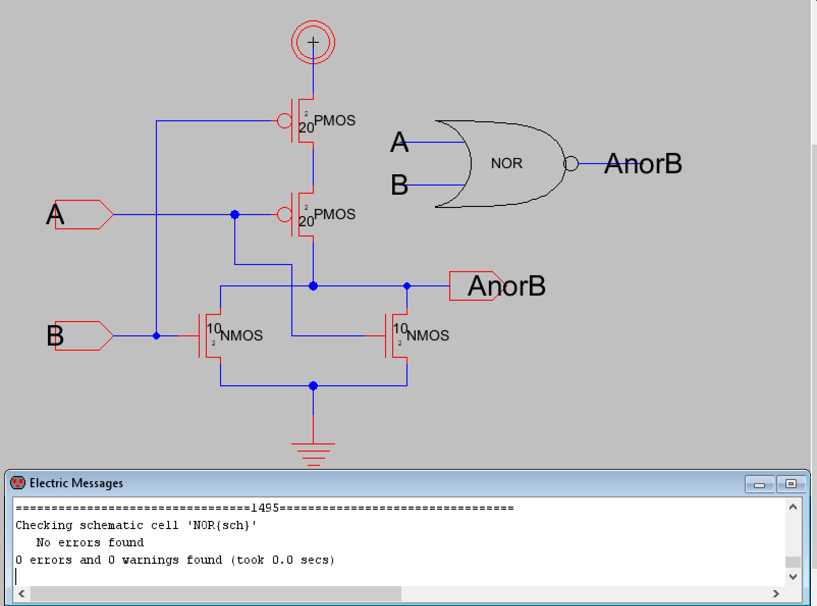
Figure 8. Schematic and icon of the NOR gate with DRC check results.
After this the simulation schematic was created to verify NOR gate
logic. Figure 9 below shows the simulation schematic while Figure 10
shows the LTSpice simulation waveform results.
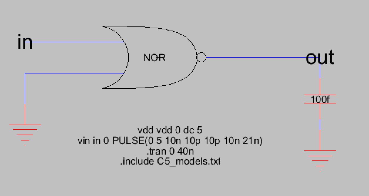
Figure 9. Simulation schematic for the NOR gate.
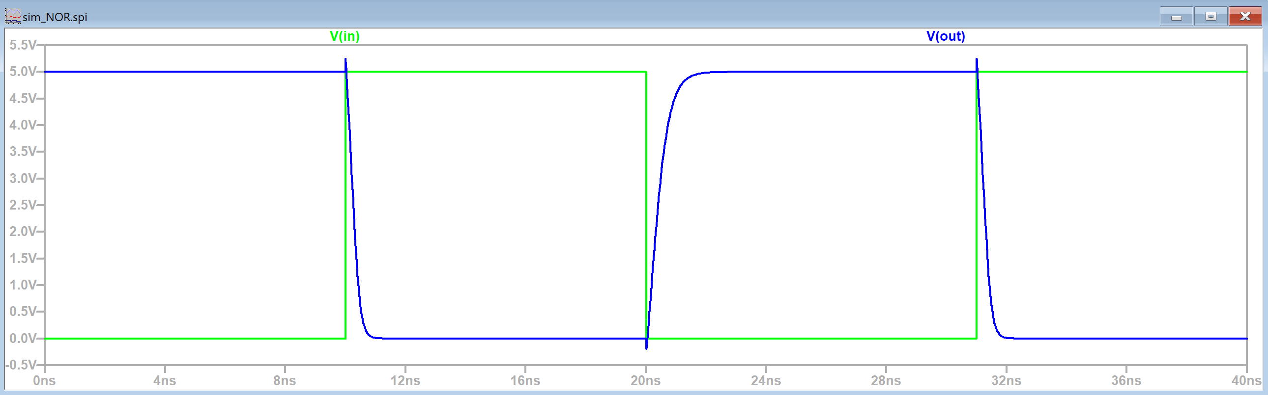
Figure 10. LTSpice simulation waveform results for the NOR gate.
Now that NOR gate logic has been verified the layout view was created.
The process was similar to the NAND gate, the appropriate nodes were
added such as the PMOS, NMOS, nAct, pAct, nWell, and pWell nodes. The
inputs and output pins were also exported. After this was done a DRC
and NCC check was performed to verify the layout would work. Figure 11
below shows the final layout view of the NOR gate and Figure 12 shows
the DRC and NCC check results.
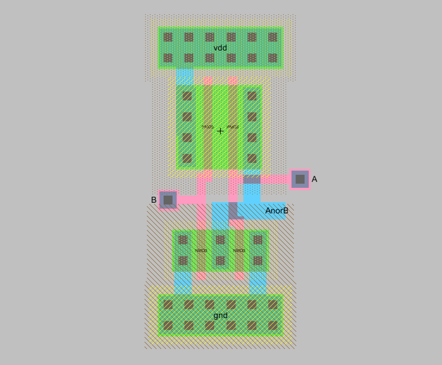
Figure 11. Final layout view for the NOR gate. All necessary connections have been made and pins were exported.
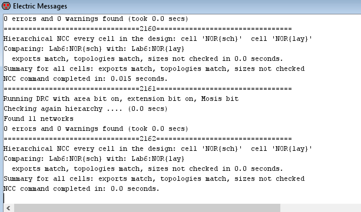
Figure 12. DRC and NCC check results for the final NOR gate layout view.
Task 3: Design, simulate, and layout an XOR gate.
The process of building the XOR gate was very similar to the previous
gates. The schematic and icon views were created first. The schematic
was more complicated than previous logic gates because the XOR gate's
boolean expression is (NOT A)B + A(NOT B) which involves an inverter
(to get NOT A and NOT B) plus the AOI logic necessary. Figure 13 which
was taken from the lab shows the AOI logic for the XOR gate. Figure 14
below shows the schematic I created for the XOR gate which included
inverting A and B to get (NOT A) and (NOT B) which were used in the
areas indicated by Figure 13.
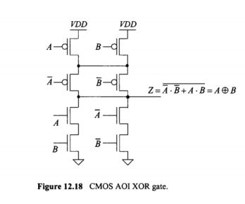
Figure 13. AOI Logic for an XOR gate which was provided for this lab. Original figure is from Dr. Baker's CMOS book pg 367.
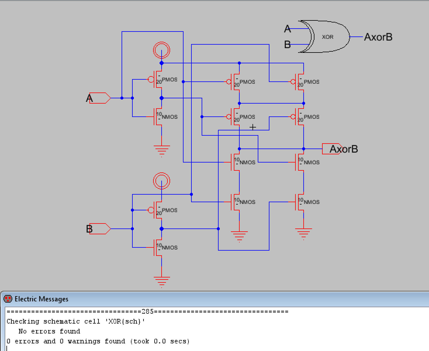
Figure 14. Schematic view for
the XOR gate. The icon can be seen in the upper right corner. The
schematic also successfully passed DRC check.
Once the schematic successfully passed a DRC check the next step was to
again create a simulation schematic to verify XOR gate logic. Two
simulation schematics were create for the XOR gate. For both simulation
schematics, one input of the XOR gate consisted of a square wave while
the other input was connected to either VDD or GND. Figures 15 and 16
show the simulation schematic and LTSpice simulation waveform for the
schematic that has B connected to VDD.
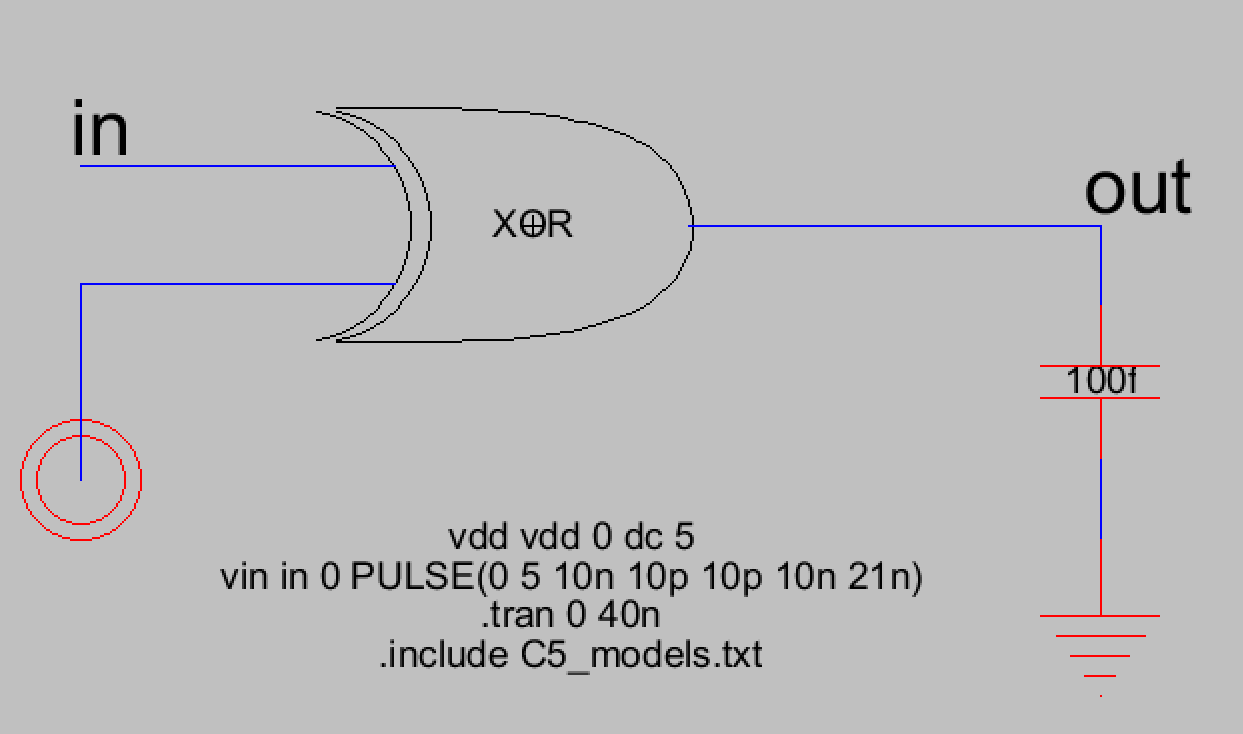
Figure 15. Simulation schematic for the XOR gate with one input being a square wave and the other input being VDD.
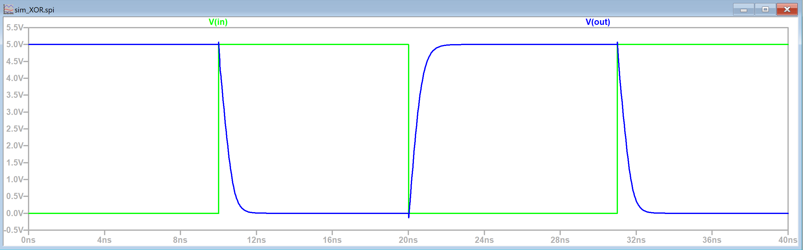
Figure 16. LTSpice simulation waveform for the XOR gate with one square wave input and one VDD input.
Figures 17 and 18 show the simulation schematic and LTSpice simulation waveform for the schematic that has B connected to GND.
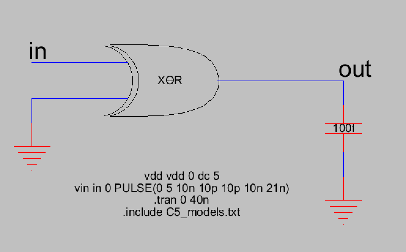
Figure 17. Simulation schematic for the XOR gate with A input connected to the square wave and the B input connected to GND.
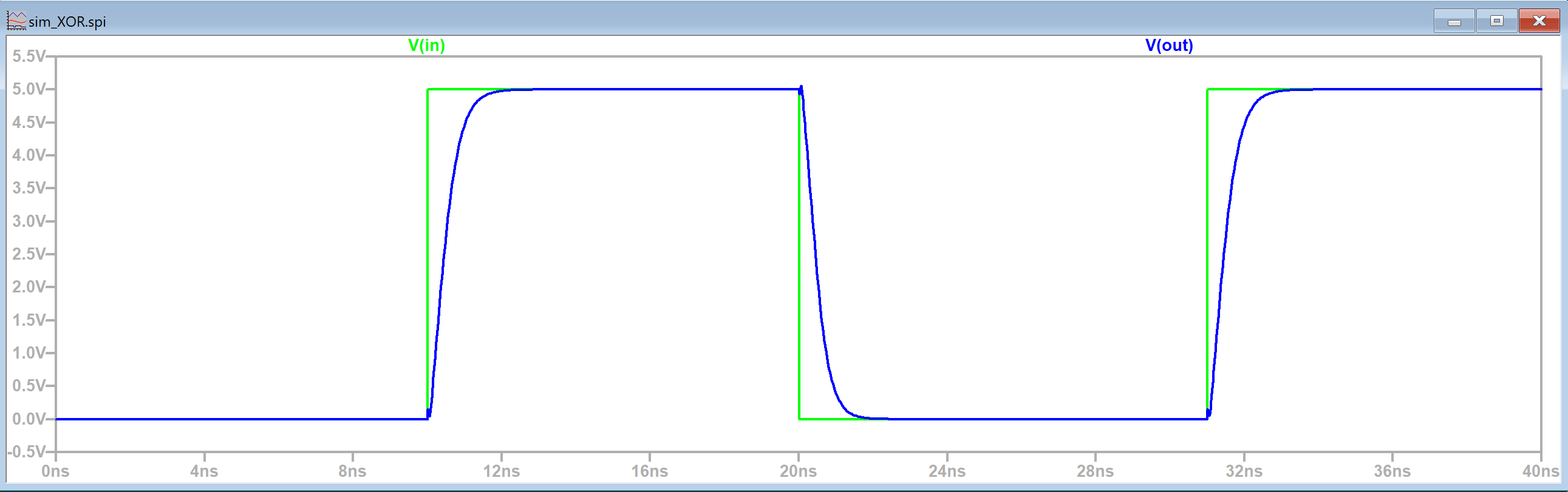
Figure 18. LTSpice simulation waveform for the XOR gate with the square wave input and GND input.
Now that the XOR gate's logic has been verified, the next step was to
create the layout view for the XOR gate. This layout view was the most
complicated so far and a stick diagram was used to assist with the
process. We were also introduced to using pure N-Well-Nodes and pure
P-Well-Nodes to avoid DRC errors in our layout design. The first step
was to add just the necessary components. So accoding to the stick
diagram shown in Figure 19, there were 5 PMOS transistors and 5 NMOS
transistors that needed to be arranged in the structure shown.
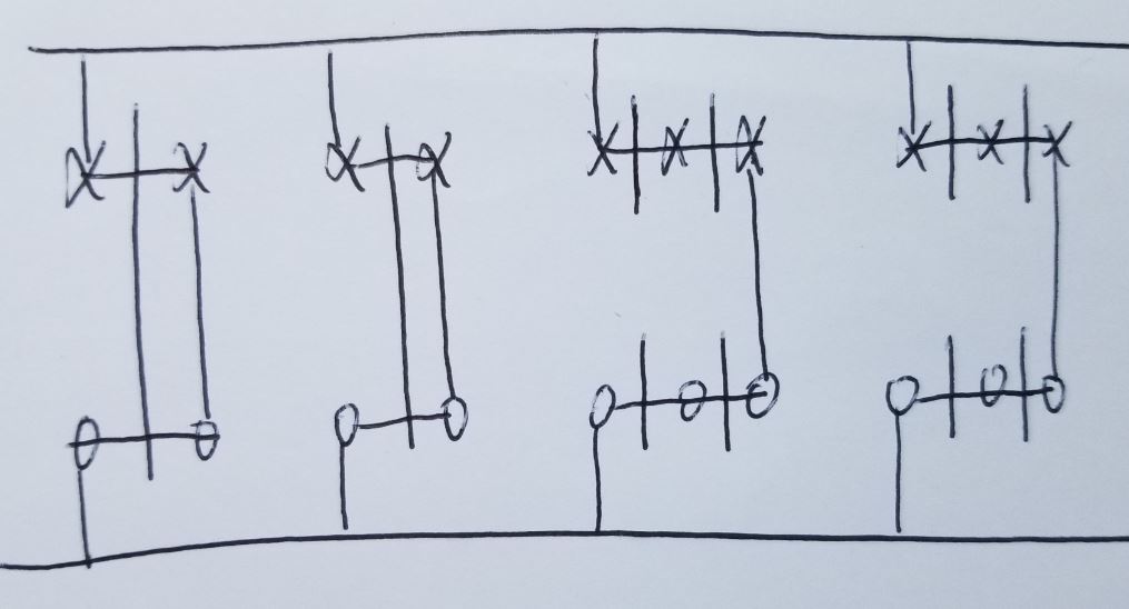
Figure 19. Stick diagram of the XOR gate with only the transistors' basic connections.
This structure was replicated in Electric VLSI to create the initial
layout view for the XOR gate shown below. Note that the channel
connections for the first set of PMOS and NMOS transistors haven't been
connected yet. At this point a DRC check was performed to verify the
initial layout was good before proceeding to make all the necessary
connections.
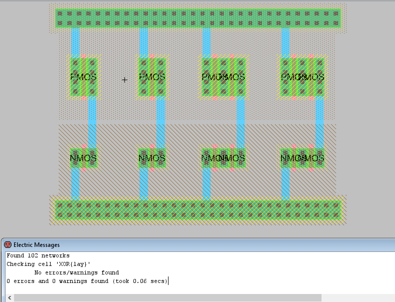
Figure 20. Initial layout view for the XOR gate. Basic connections have
been made and pure N-Well and pure P-Well nodes were used.
This next stick diagram shows all the connections that are
necessary. Using this stick diagram, the schematic, and the image of
how the XOR gate layout should look, I was able to finish the XOR
layout view and pass the required DRC and NCC checks. Figure 21 shows
the stick diagram of connections, Figure 22 is the lab's image of the
final XOR gate layout, and Figure 23 shows my final layout view for the
XOR gate along with DRC and NCC check results. The lab's provided image
of the finished XOR gate layout looks similar to mine with a few minor
differences. The main two differences are that 1) I made the connection
from the 1st PMOS channel to the 3rd PMOS channel use less space and 2)
the AxorB output shown in Figure 22 does not match the location of the
AxorB output shown in the stick diagram and the schematic. The AxorB
output was moved to the metal2 connection that can be seen in Figure 23.
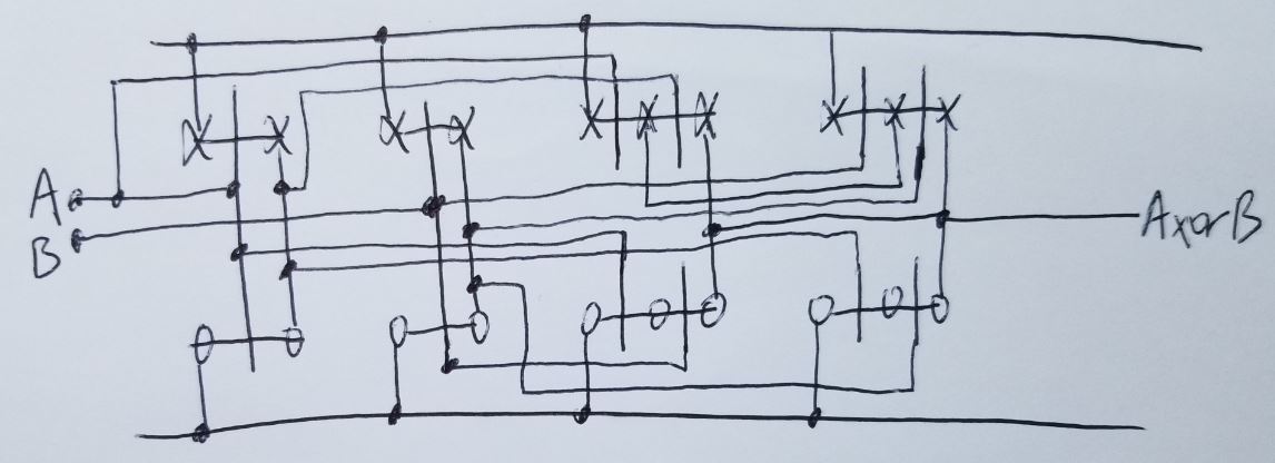
Figure 21. Stick diagram showing all of the necessary connections to be made.
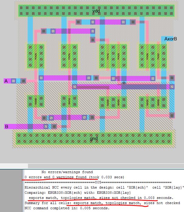
Figure 22. What the XOR gate layout view should resemble according to the lab instructions.
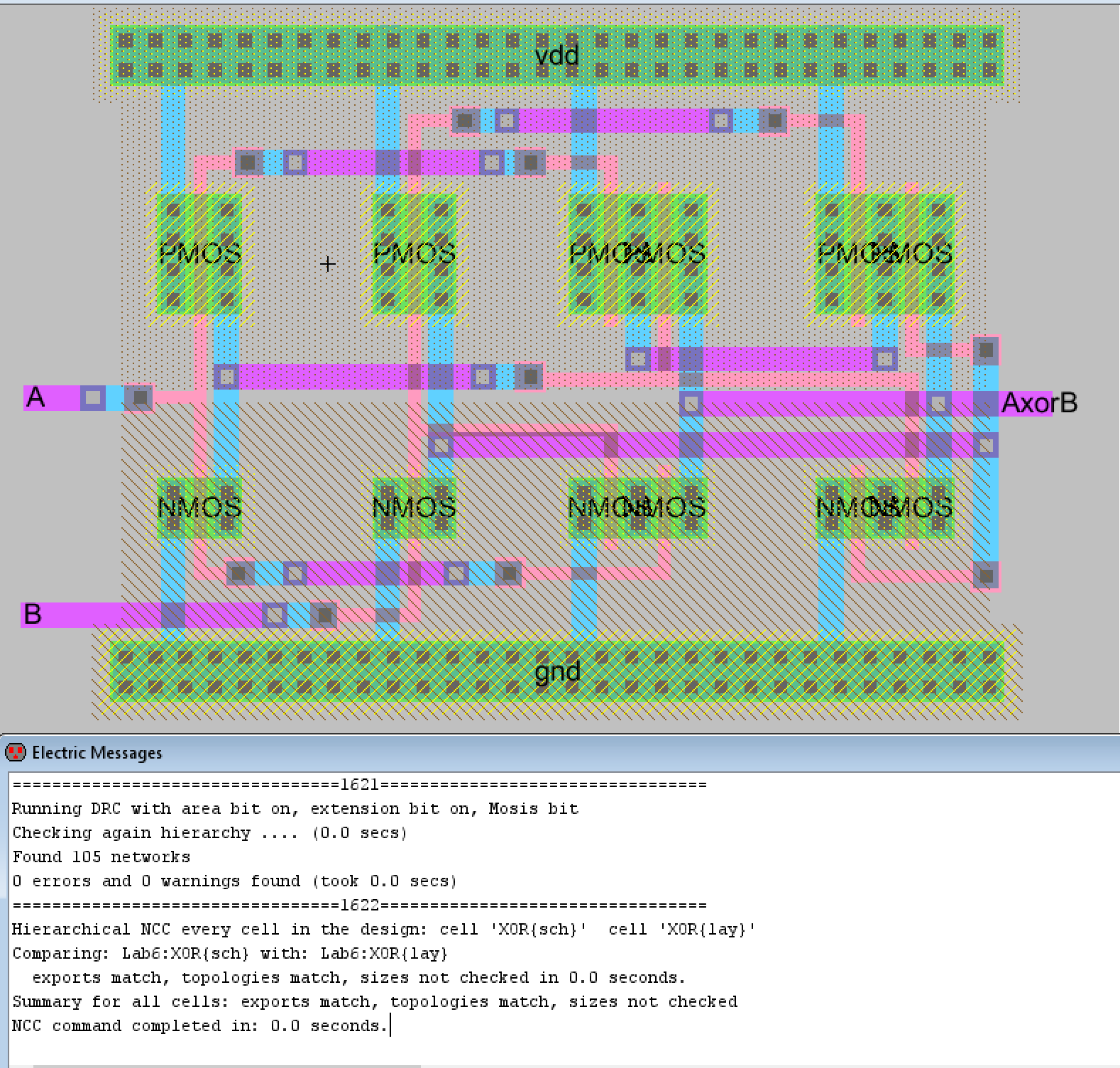
Figure 23. My final XOR gate layout view with DRC and NCC check results.
Task 4: Design, simulate, and layout a Full Adder.
In task 4 we combined the gates created so far, the NAND, the NOR, and
the XOR gates to create a full adder. The schematic for this was not
very complicated however, the layout view would increase the complexity
by requiring us to use the previous layouts in one large layout. We
started this task like the others, first the schematic view and icon
view were created, a DRC check performed, and the logic verified before
moving onto the layout view. The inverter schematic, icon, and layout
had to be copied over from our previous Lab 5.
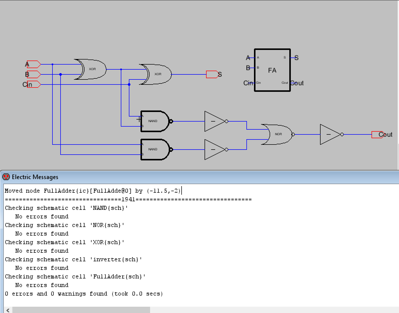
Figure 24. Schematic view with the full adder's icon and DRC check results.
The first simulation used a square wave for A and B inputs while the
carry in (Cin) input was connected to ground. This would be adding when
there was no carry present. The simulation schematic can be seen in
Figure 25 below and the LTSpice simulation waveform can be seen in
Figure 26.

Figure 25. Simulation schematic for the full adder with no carry in.
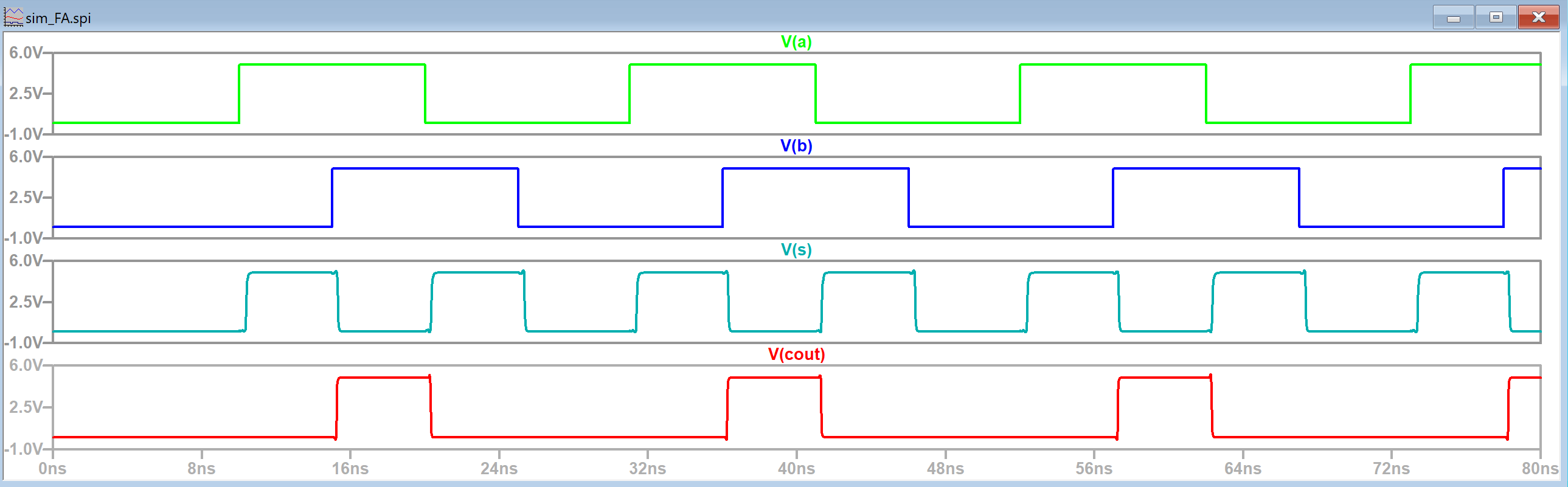
Figure 26. LTSpice simulation waveform for the full adder with no carry in.
After this the next simulation schematic verified that the full adder
was functioning properly with a carry in. The carry in was simply set
to high instead of to ground. Figure 27 shows the simulation schematic
while Figure 28 shows the LTSpice simulation waveform. It was noted
that the carry out output had glitches due to the time delay of the
full adder as seen in Figure 28.
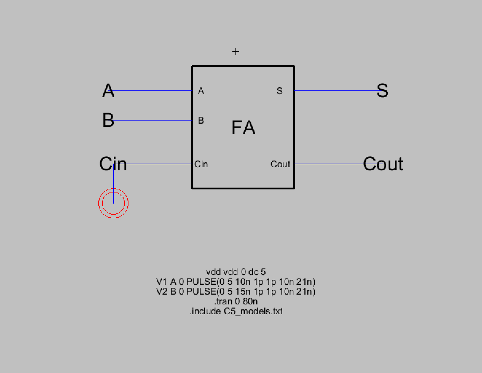
Figure 27. Simulation schematic for the full adder with a carry in.
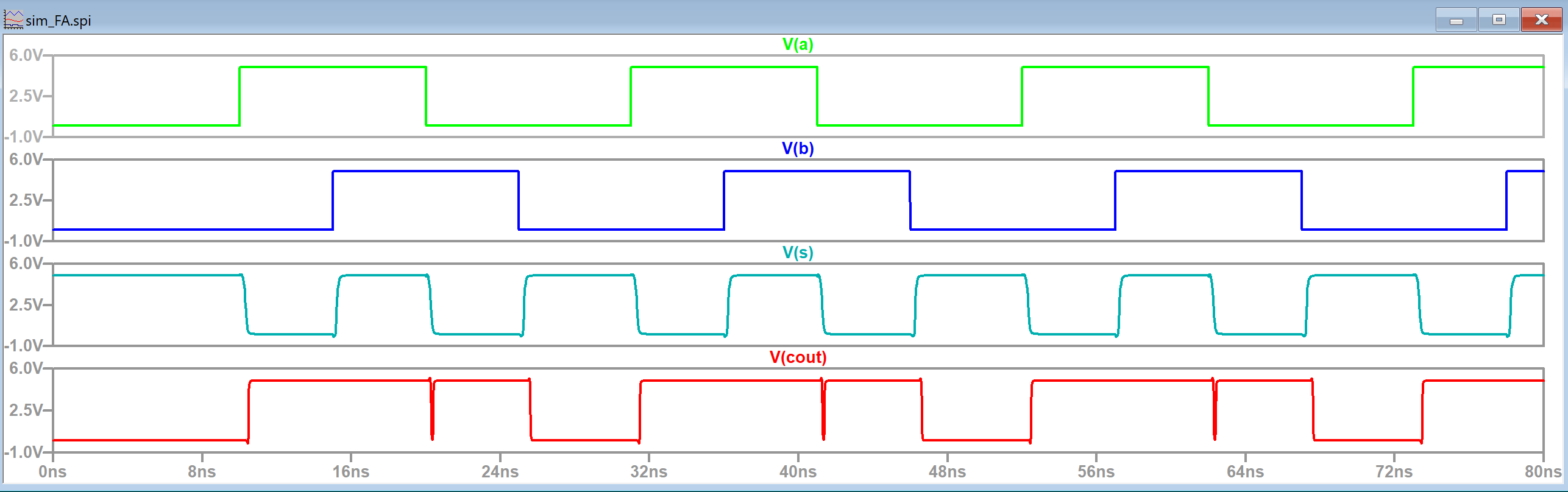
Figure 28. LTSpice simulation waveform for the full adder with carry in.
The logic has now been verified so the next step was starting on the
layout view for the full adder. At this point it was recommended that
we adjust the layout views of the other gates so that the VDD nWell and
GND pWell nodes were all at a consistent height as shown in Figure 29.
I decided to base the y values for these components on where they were
located for the XOR gate. I ended up setting each VDD nWell to Y
position 35 and each GND pWell to Y position -68.5. Figure 29 shows the
adjusted NAND gate. The other gates were similarly edited.
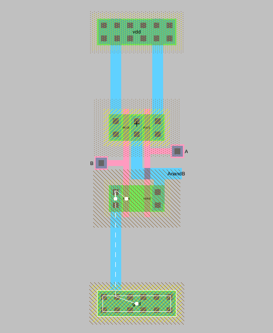
Figure 29. The NAND gate that has had its VDD nWell and GND pWell nodes positioned to the correct y values.
I began the layout view of the full adder by placing two XOR gates
together and making the connections seen in the schematic shown in
Figure 24. I made sure to use metal3 for the input pins and output pins
and ran DRC checks after every connection to ensure errors in the
layout wouldn't pile up near the end. Figure 30 shows the first part of
the full adder's finished layout view.
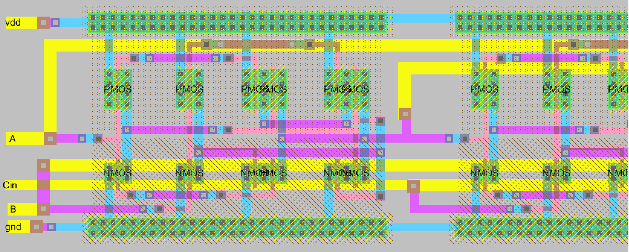
Figure 30. The first portion of the full adder layout view. One XOR gate can be seen along with half of the next one.
After this I decided on which of the NAND gates to do first. I decided
to the NAND gate that had the A and B inputs first so that the A and B
metal3 connections wouldn't have to travel so far. I placed an inverter
after it and then the next pair of NAND gates and inverters. Figure 31
shows the half of the first NAND gate, its inverter, the second NAND
gate, its inverter, and then finally the NOR gate along with its
inverter.
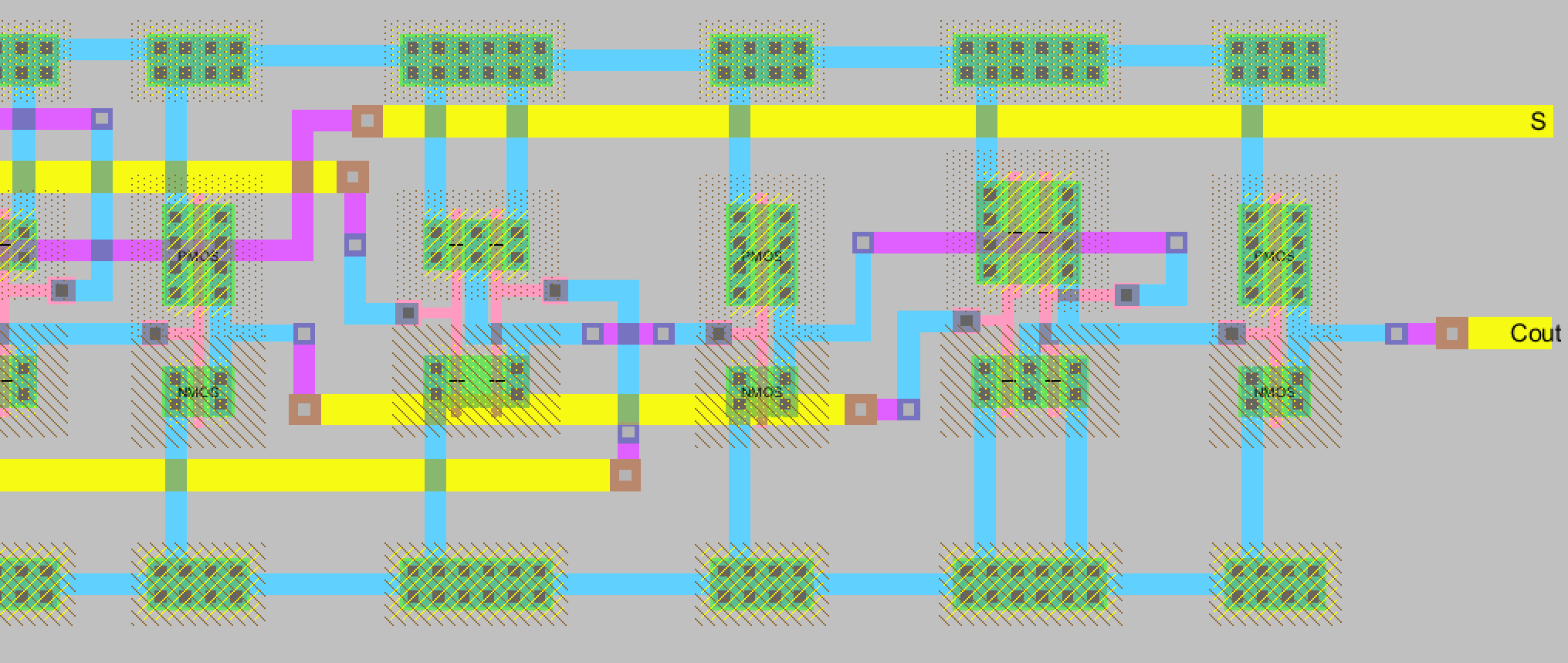
Figure 31. The final portion
of the full adder layout view. It consists of a NAND gates, Inverters,
and a NOR gate in the order noted above.
The whole entire layout view can be seen below. The full image will also appear if clicked on.
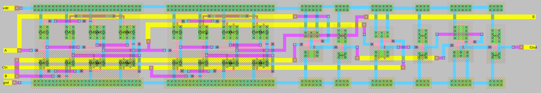
Figure 32. The entire full adder layout view. It can be viewed in more detail if clicked on.
This full adder layout view successfully passed DRC and NCC checks
after some troubleshooting. The results can be seen below in Figure 33
along with a view of the middle portion of the layout view.
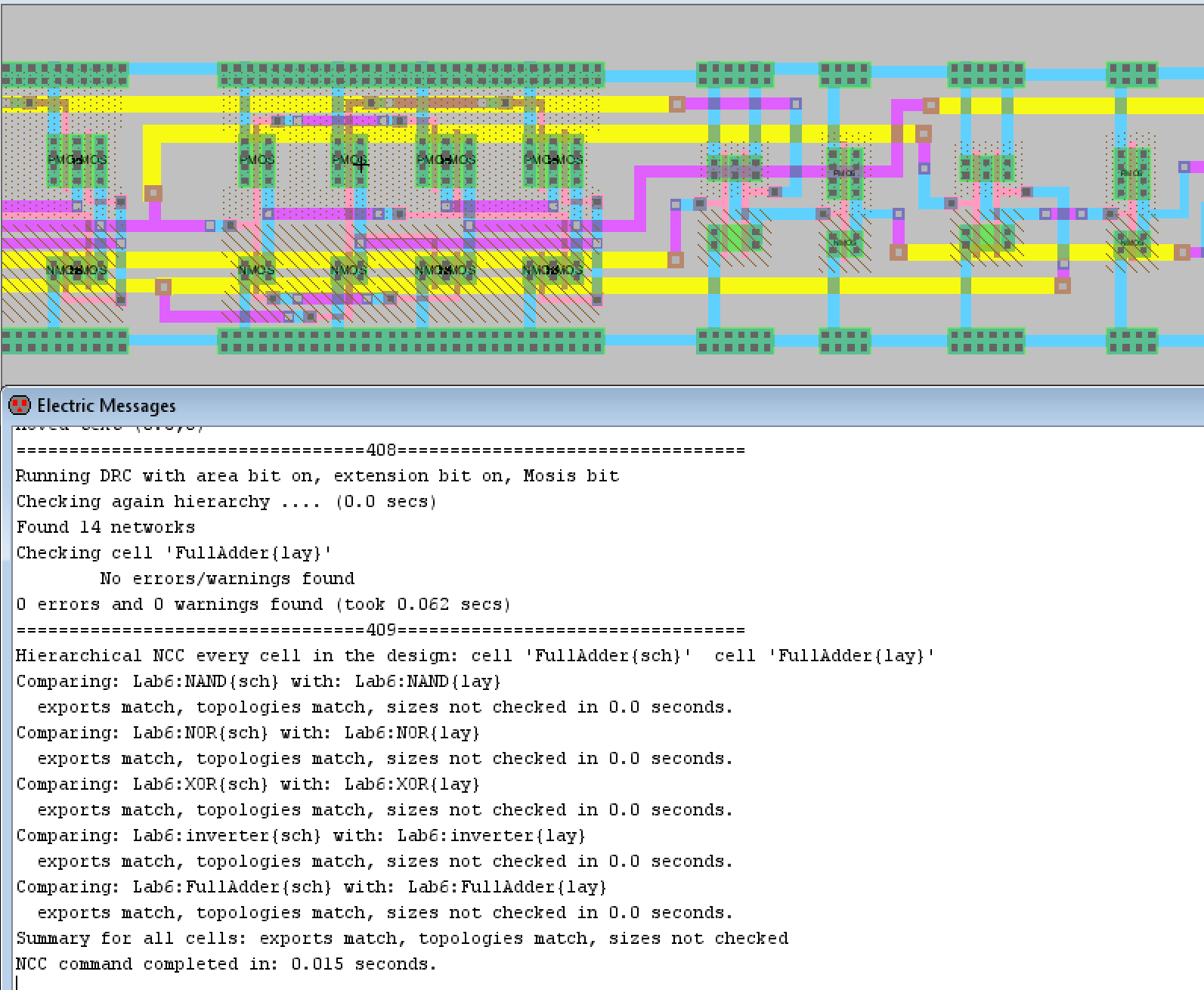
Figure 33. DRC and NCC check results for the full adder layout view. The middle portion of the full adder layout is also seen.
Discussion
This lab was very fun to work on. I liked creating the logic gates and
then combining them together to create the full adder at the end. I
didn't have any issues when creating the NAND and NOR gates but I did
have to figure out why I was getting errors for the XOR gate and Full
Adder layout views.
For the XOR gate the main issue I had was placing the AxorB output
since the image shown in the lab placed it differently from the stick
diagram. I kept getting NCC check results that said the topologies
didn't match and it was due to an extra wire not seen in the schematic.
I ended up solving it by going off the stick diagram for that output
pin, which matched how the schematic looked, and it was able to pass
NCC.
For the Full Adder layout, the main issue I ran into was making sure
the connections going into the NAND gates matched what the schematic
showed. For a while I wasn't able to figure out the issue since the NCC
errors window only said that there were 4 mismatched parts. It said
there was a NAND@0 and NAND@1 part in the schematic but not in the
layout but then it repeated the error for the layout view. It would
also say there was a NAND@0 and NAND@1 part in the layout view but not
in the schematic view, which I didn't understand why. It seemed like
Electric VLSI wasn't able to detect I was using the NAND gate's layout
in my layout view or vice versa, its icon in the schematic view. I
tried editing the names to NAND@2 etc. to see if it would detect it
then but then similar errors happened for the inverters. I fixed the
issue by going over the connections being made over and over until I
saw that the second NAND gate, the one that had one input from the
first XOR gate's output and the second input from the Carry in (Cin)
input, had the signals going into the wrong NAND gate inputs. I had to
make the 1st XOR gate's output go into the B input of the NAND gate and
the Carry in input go into the A input where before it was the other
way around. I initially made the connections that way because the
connections were looked more straightforward to make. Finally the layout view passed NCC checks!