CE351 2020 Fall
Lab 1: Power Supply
Sophie Turner
sjturner@fortlewis.edu
Power Supply and DC Regulators on a PCB for MCUs
1. Introduction
The purpose of this lab was to design a power supply that outputs 3.3V,
5V, and 1A or 3A. Eagle software was used to design a printed circuit
board (PCB) to use
for future projects.
2. Materials and Methods
Eagle
software was used to create the schematic and layout of the PCB. SparkFun
Library was installed to add parts to the schematic. A new library was created to make custom parts for the PCB.
Seven new devices were created for
the PCB: 4.7uF capacitor, 33uF capacitor, Schottky Diode, 33uH inductor, 47uH
inductor, LM2596_5V, and LM2596_3.3V. The parts were organized and wired on
both the schematic and board. DRC checks were run throughout the process
to catch errors. A Gerber file was created and put into an online Gerber
viewer to locate mistakes.
For a more detailed methods section go to http://www.yilectronics.com/Courses/CE351_Microcontrollers/f2020/lectures/powerSupply/powerSupply.html .
3. Results
Custom devices were created for this lab: 4.7uF capacitor, 33uF capacitor, Schottky Diode, 33uH inductor,47uH
inductor, LM2596_5V, and LM2596_3.3V. The custom devices are shown in figures 1-5.
The 4.7uF capacitor has a 8.3x8.3mm footprint and the 33uF capacitor has a 8.3x10mm footprint.
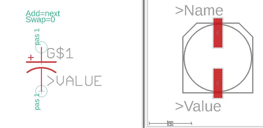
Figure 1. Footprint and symbol for the 4.7uF and 33uF capacitors.
The 33uH inductor and 47uH
inductor have the same footprint and symbol.
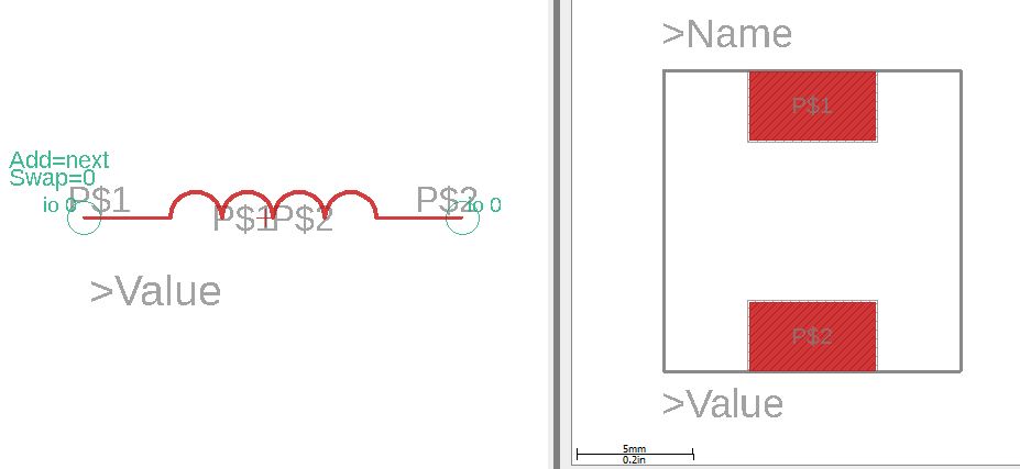
Figure 2. Footprint and symbol for the 47uH and 33uH inductor.
The LM2596_5V and LM2596_3.3V DC-DC buck converters also have same footprint and symbol.
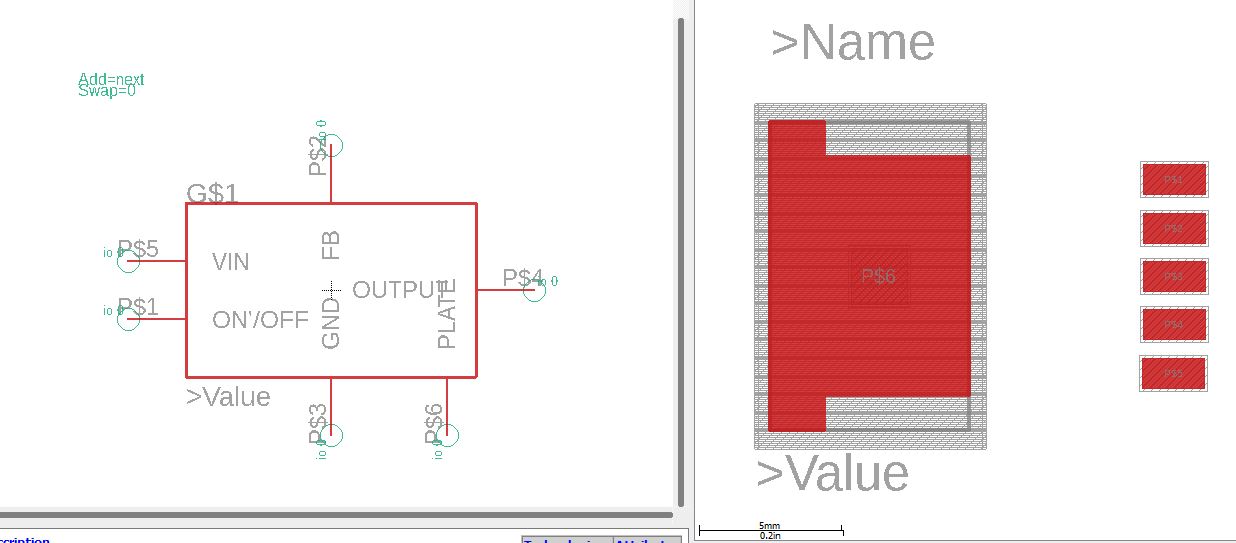
Figure 3. Symbol and footprint for the LM2596_5V and LM2596_3.3V DC-DC buck converters.
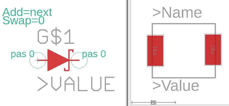
Figure 4. Symbol and footprint for the Schottky diode.
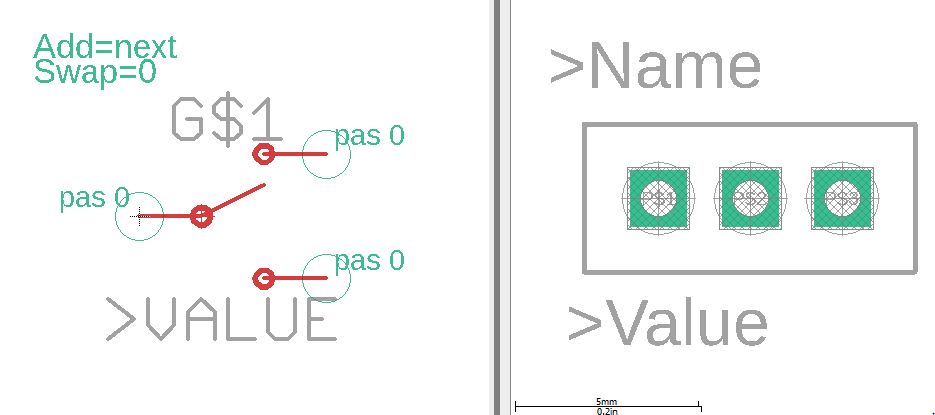
Figure 5. Symbol and footprint for the switch.
In Figure 6 the schematic contains parts from SparkFun Library.
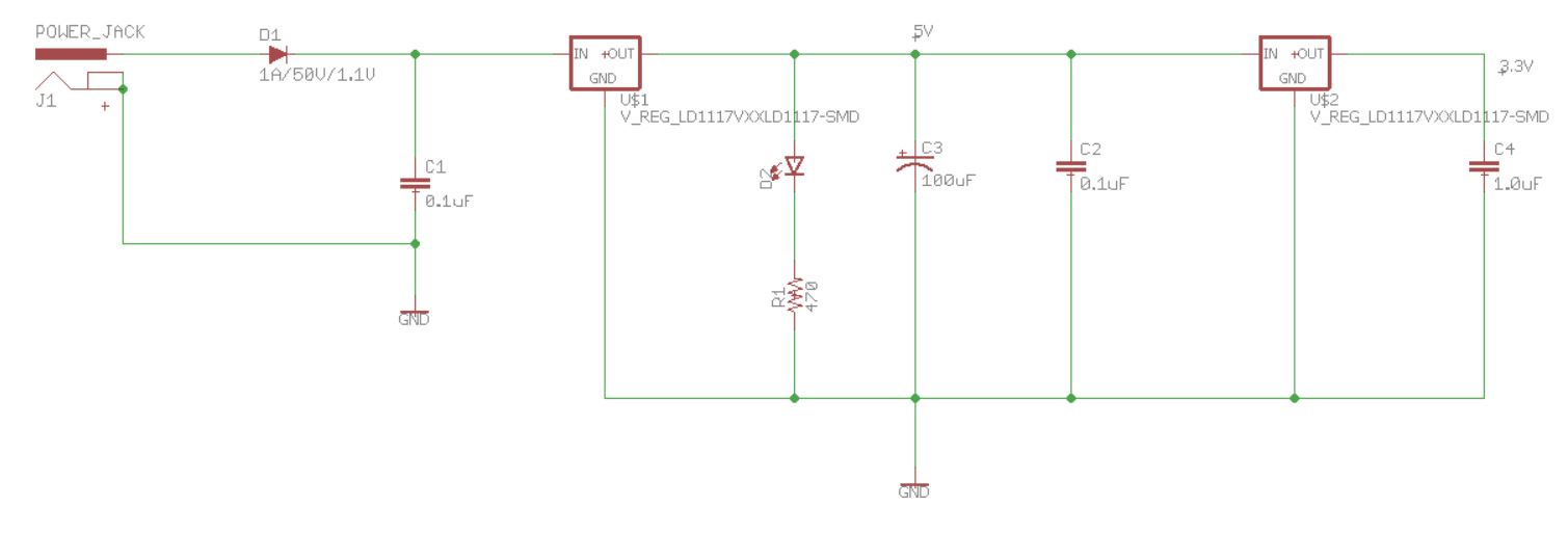
Figure 6. 5V and 3.3V schematic with parts from SparkFun Library.
Figure 7 includes all parts for the PCB manufacturing, including the custom parts that were created for this lab.
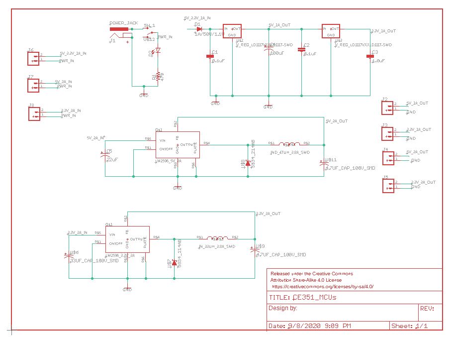
Figure 7. Final schematic of the power supply.
All the devices were organized and labeled on the board
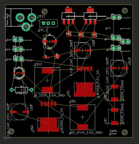
Figure 8. BRD view
The board was wired using Autorouter.
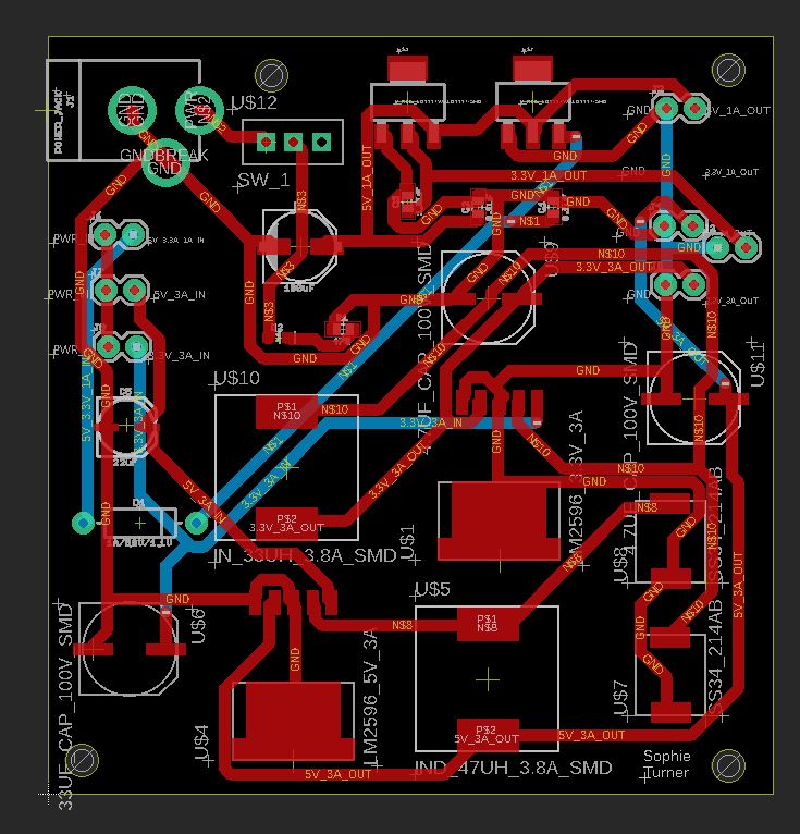
Figure 9. Routed BRD view.
After routing a copper layer was laid. DRC was run to check for errors; no errors occurred.
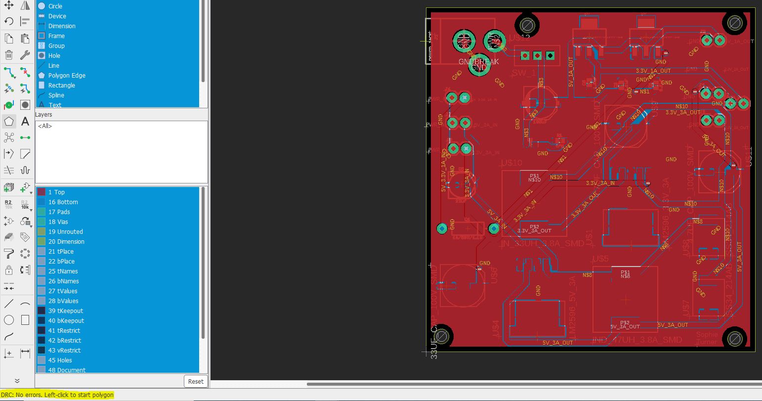
Figure 10. BRD view with copper pour and DRC check.
PCB Investigator online Gerber viewer was used to check for any mistakes before fabrication.
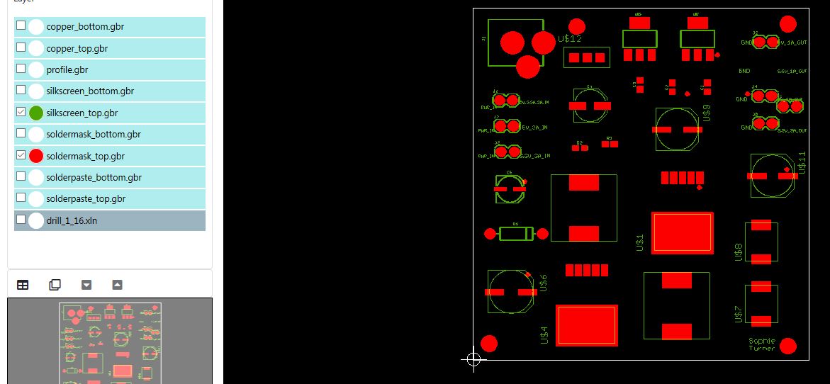
Figure 11. PCB investigator Gerber viewer of the final PCB with silkscreen_top and soldermask_top.
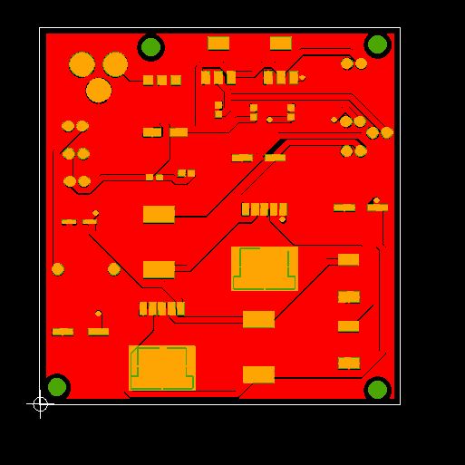
Figure 12. PCB investigator Gerber view with copper_top and soldermask_top
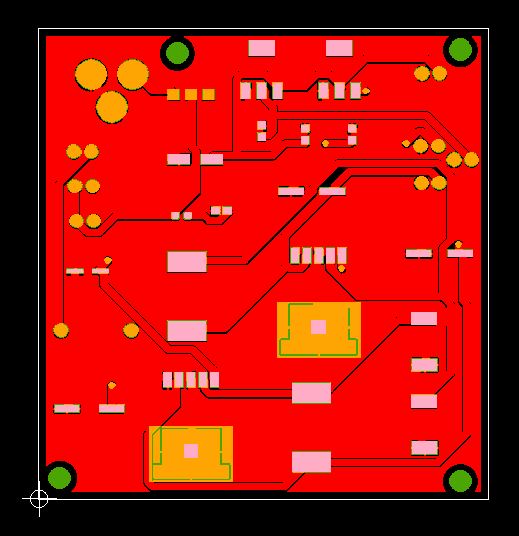
Figure 13. PCB investigator Gerber view with copper_top, soldermask_top and silkscreen_top.
After soldering the parts on the board, the output voltage was tested for all four pin.
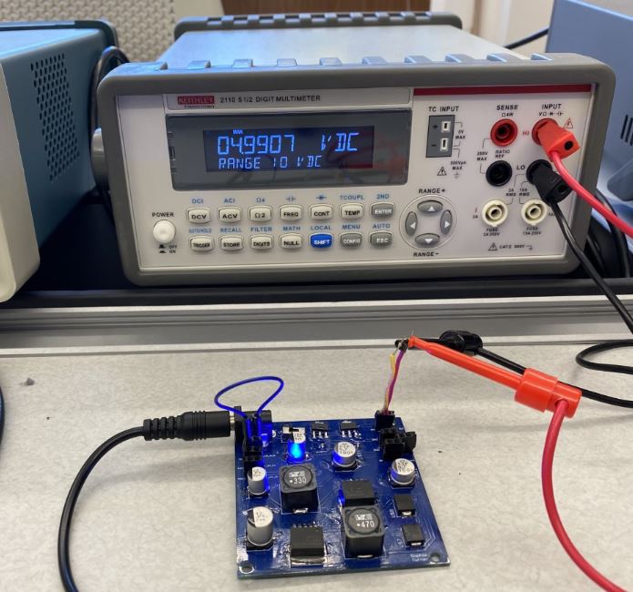
Figure 14. Testing my PCB for an output of 5V and 1A.
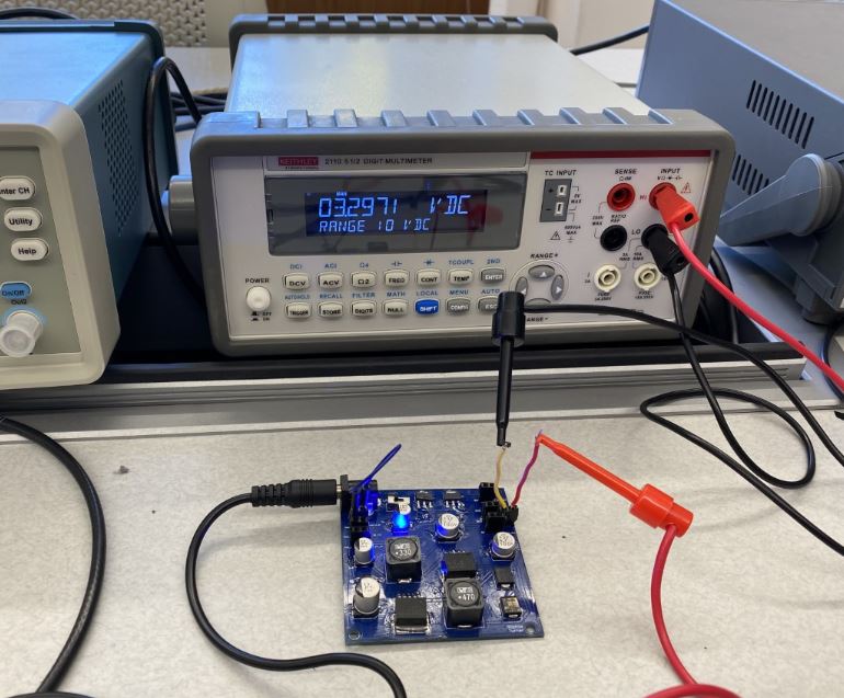
Figure 15. Testing my PCB for an output of 3.3V and 1A.
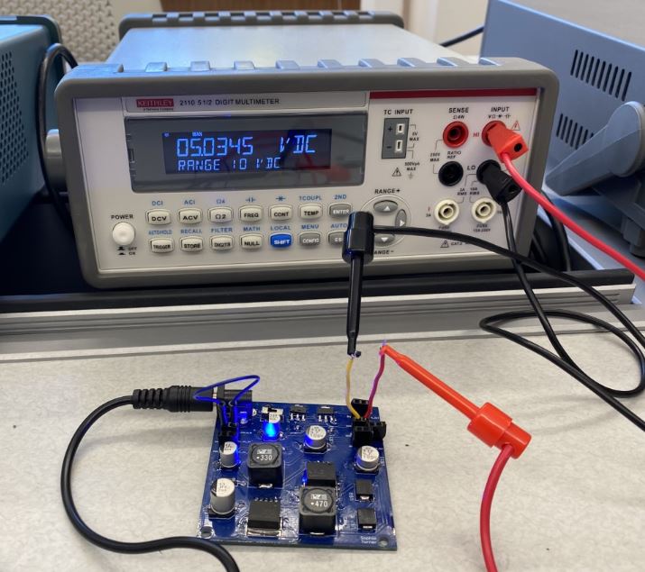
Figure 16. Testing my PCB for an output of 5V and 3A.
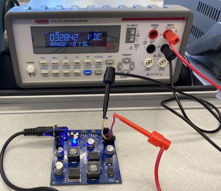
Figure 17. Testing my PCB for an output of 3.3V and 3A.
4. Discussion
Eagle
software was used to design a PCB to output 5V, 3.3V and 1A or 3A. After running
into many complications in the process, the DRC is error free.
This lab allowed
me to become very familiar with Eagle and experience the process of designing a
PCB.
After designing the board, the Gerber file was sent for board
fabrication. All the parts were soldered on and then the output
voltage was tested for each pin. My board outputs the correct voltage
as expected.