ENGR338
2021 Spring
Lab 9: Design a Simple 8-bit ALU
Sophie Turner
sjturner@fortlewis.edu
Design a Simple 8-bit ALU
1. Introduction
The purpose of this lab to build an 8-bit
arithmetic logic unit (ALU) in ElectriVLSI. The ALU can perform AND, OR,
addition, and subtraction operations. The ALU was created by combining gates
created in previous labs: 8-bit MUX, 8-bit AND, 8-bit OR, and inverter. An
8-bit inverter layout, icon, and schematic were also created for this design. A
schematic, layout, and icon were created for the ALU.
2. Methods
ElectriVLSI was used to create the design for ALU. LTSpice was
used to simulate the logic of the 8-bit ALU. For more detailed
methods go http://yilectronics.com/Courses/ENGR338L_CE/lab9_ALU/Lab9.html
3. Results
Task 1.
A schematic and layout of an 8-bit ALU was
created. A simulation was run in LTSpice to simulate the ALU functionality. The
8-bit ALU schematic was created by combining three 8-bit MUX, 8-bit AND, 8-bit
OR, 8-bit inverter and three short 20/10 inverters. An 8-bit schematic,
layout, and icon was created to finish the lab. Buses were used to create the
schematic. DRC and NCC checks were run throughout the process.
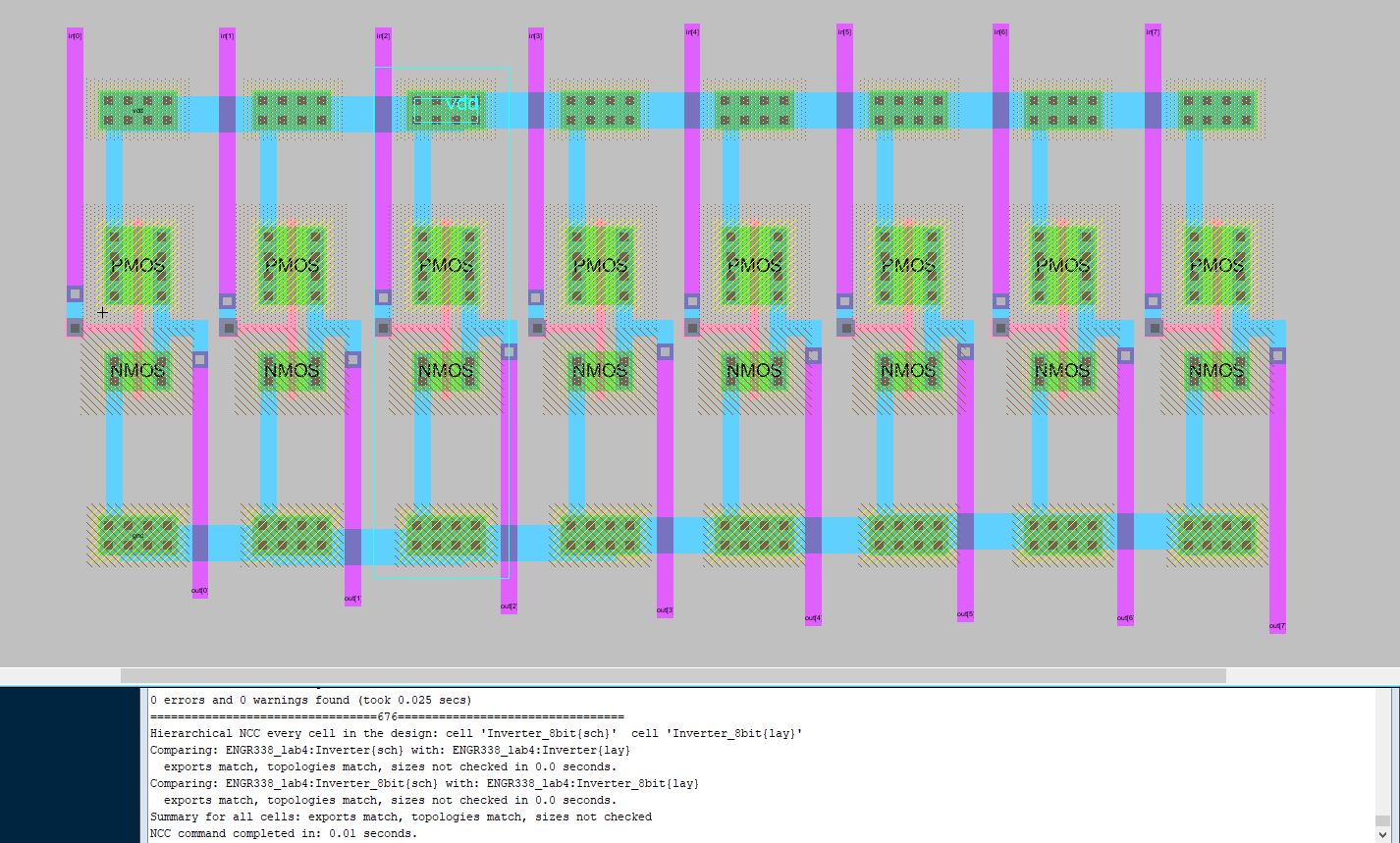
Figure 1. 8-bit inverter layout.
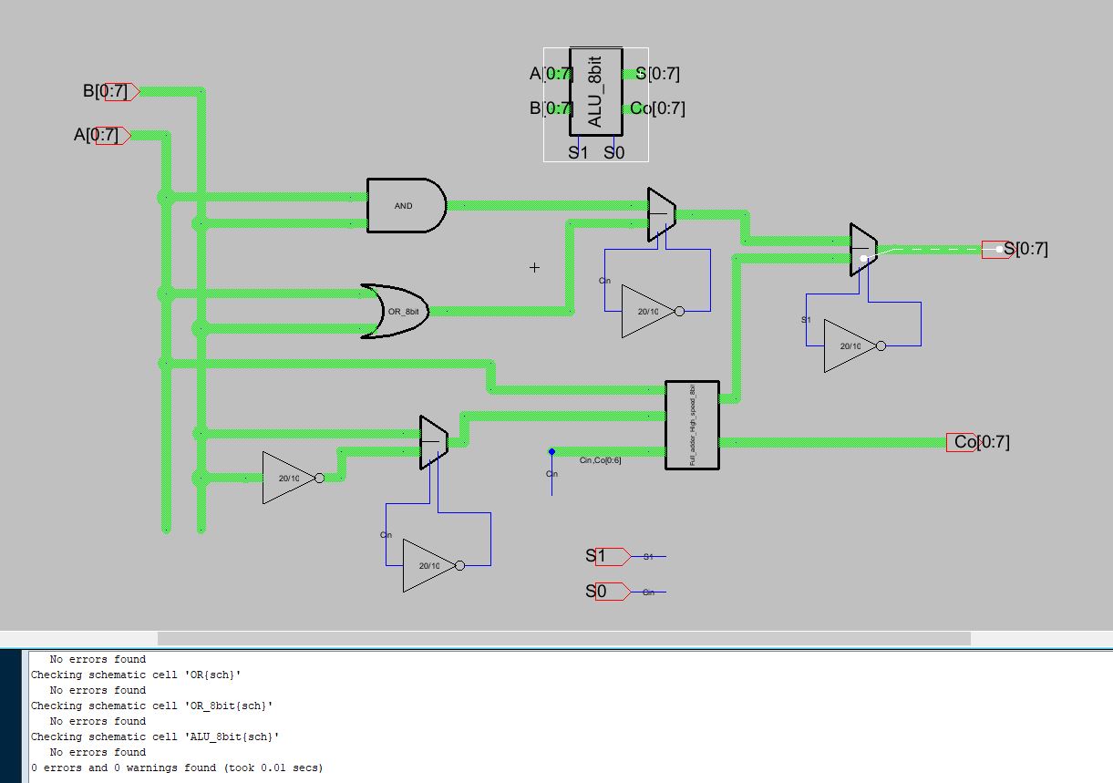
Figure 2. 8-bit ALU schematic and icon.
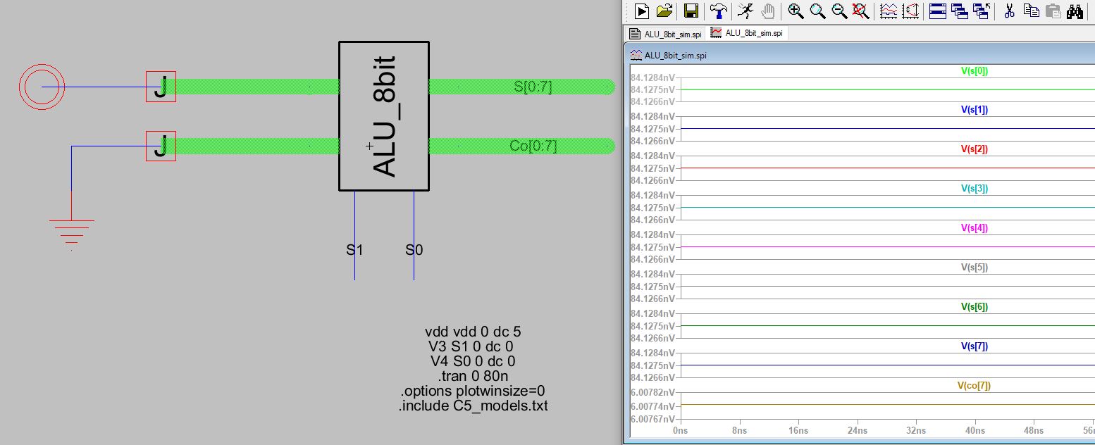
Figure 3. LTSpice simulation of the ALU AND operation. S1S0=00.
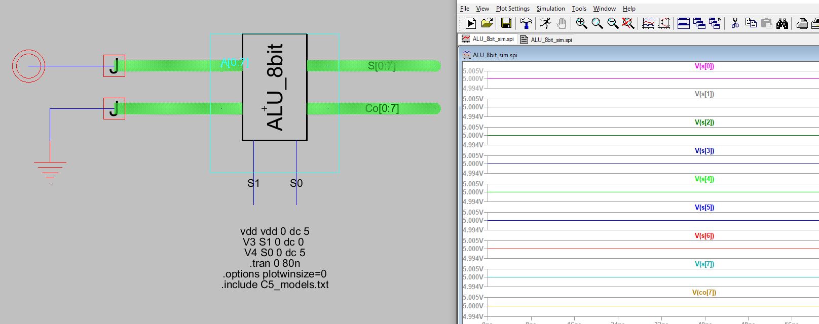
Figure 4. LTSpice simulation of the ALU OR operation. S1S0=01.
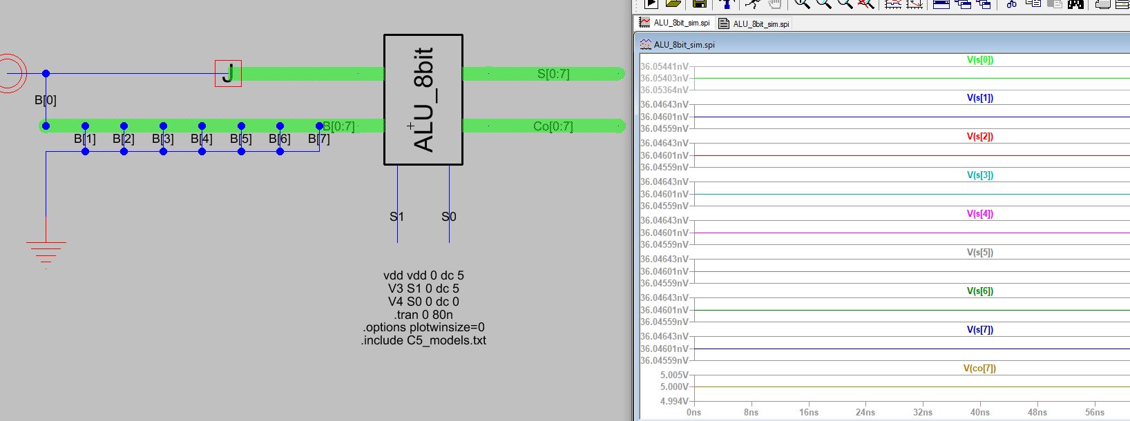
Figure 5. LTSpice simulation of the ALU add operation. S=0000 0000, Co=1.
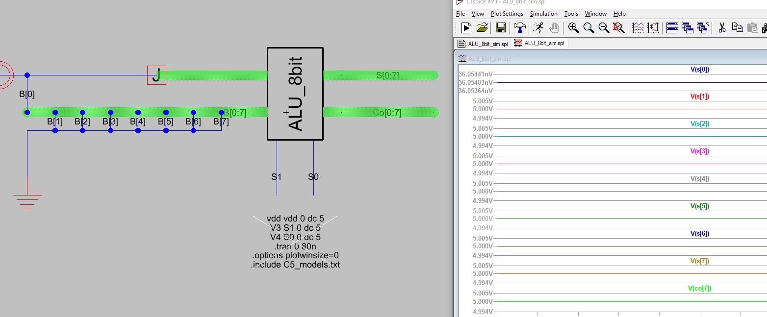
Figure 6. LTSpice simulation of the ALU subtraction operator.
Task 2.
The ALU layout was created by combining three 8-bit MUX, 8-bit AND, 8-bit OR, 8-bit inverter and three short 20/10 inverters.
DRC checks were run throughout the process, and a final NCC check was
performed to ensure the layout was correct. The ALU schematic was
revised to export only Co[7] as seen in Figure 9.
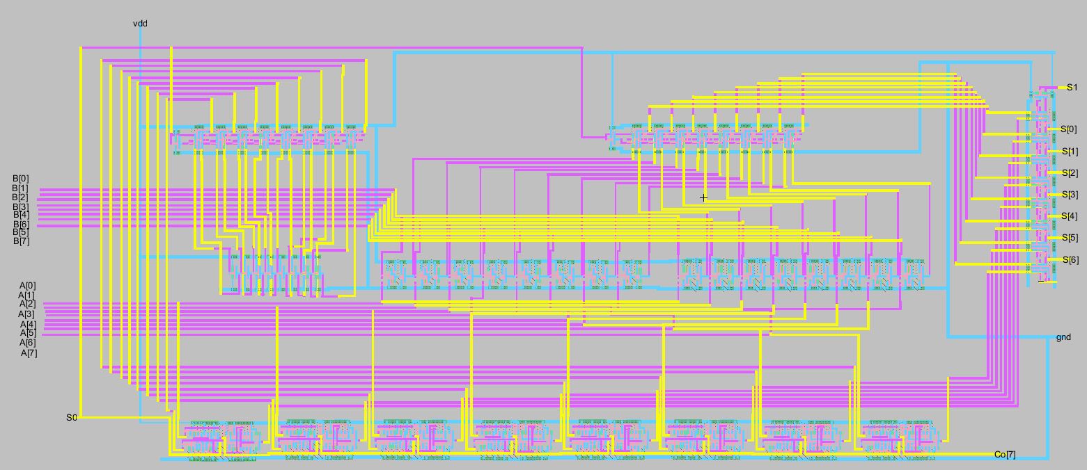
Figure 7. 8-bit ALU layout.
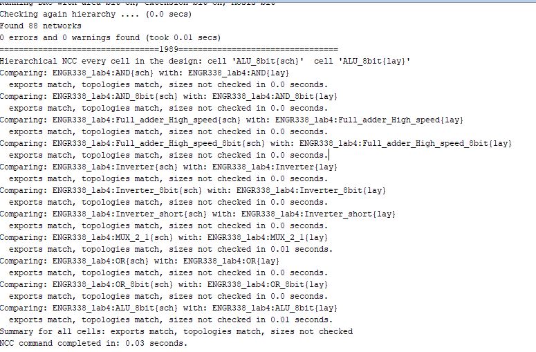
Figure 8. NCC and DRC check for the 8-bit ALU layout.
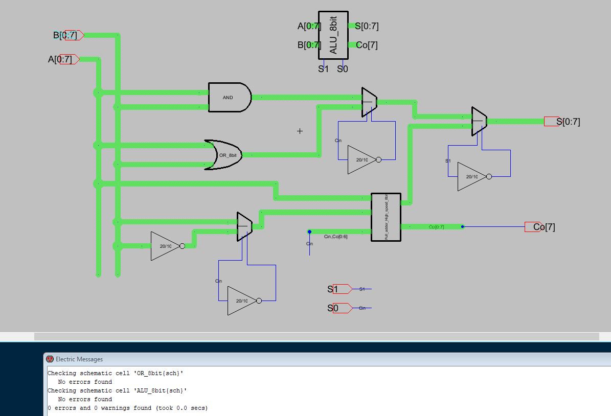
Figure 9. 1-bit high speed full adder simulation in LTSpice.
2. Discussion
This lab allowed me to gain more experience
using ElectriVLSI. The lab was implemented successfully. I was able to create
the schematic and layout for 8-bit ALU. This lab allowed all the components built
through the semester to be implemented together to create a more complex
design. Wiring all the layouts together was tedious. With more practice and
experience the more complex layout can be cleaner. The labs helped me gain experience
in designing in ElectriVLSI. Now I feel comfortable creating layouts,
schematics, and icons for different components.