ENGR338
2021 Spring
Lab 8: Design a MUX, and a High Speed Full Adder
Sophie Turner
sjturner@fortlewis.edu
Design a MUX, and a High Speed Full Adder
1. Introduction
The purpose of this lab to build an 8-bit MUX
and to build an 8-bit high speed full adder in ElectriVLSI. MOSFET transistors
were used to create a multiplexer (MUX). An 8-bit MUX was created using buses.
A schematic and layout of a 1-bit high speed full adder were created. The 1-bit
was combined to make an 8-bit high speed full adder. Simulations were run to
verify the logic on LTSpice.
2. Methods
ElectriVLSI was used to create the designs for MUX and high speed full adder. LTSpice was
used to simulate the logic of the 8-bit multiplexer and 8-bit high speed full adder. For more detailed
methods go http://www.yilectronics.com/Courses/ENGR338L_CE/lab8_MUX_FAII/Lab8.html
3. Results
Task 1.
A
schematic and layout of a 2:1 mux were
created. DRC checks were run throughout
the process, and a simulation was run in LTSpice. The 8-bit mux
schematic was created by putting 8 icons together and by using buses.
The layout was also created using 8 subcells. LTSpice was used to
simulate the logic.
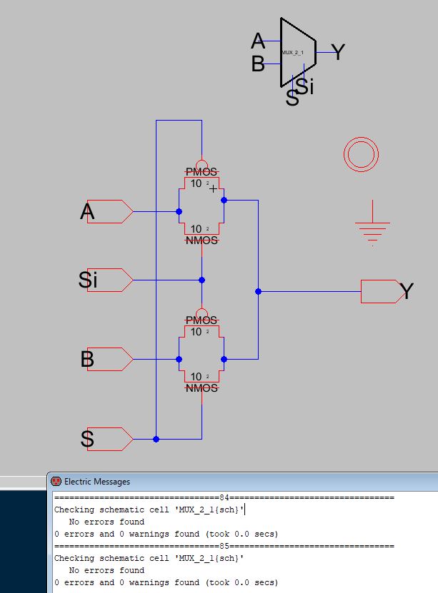
Figure 1. MUX schematic
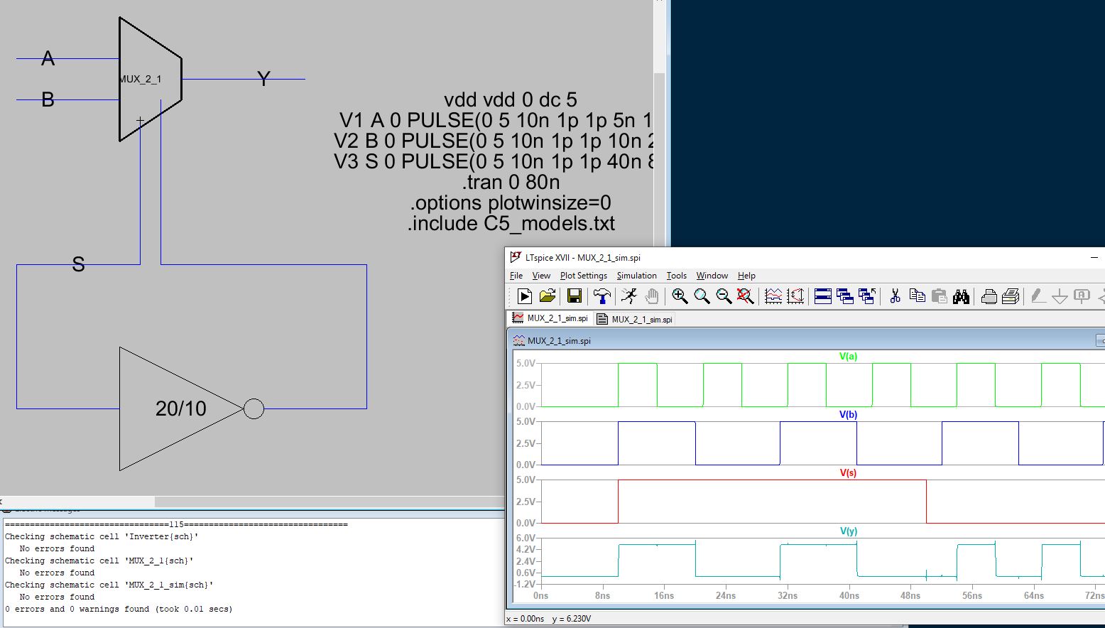
Figure 2. Simulation in LTSpice of a 2:1 MUX.
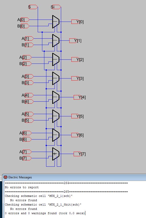
Figure 3. 8-bit 2:1 mux schematic.
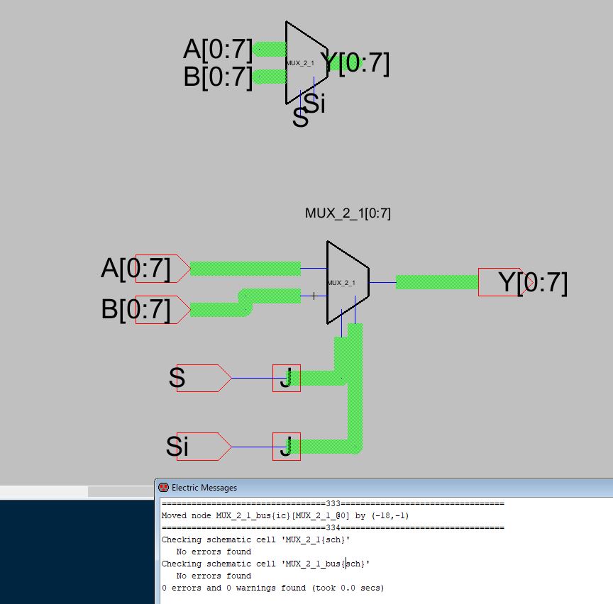
Figure 4. 8-bit 2:1 mux schematic using buses.
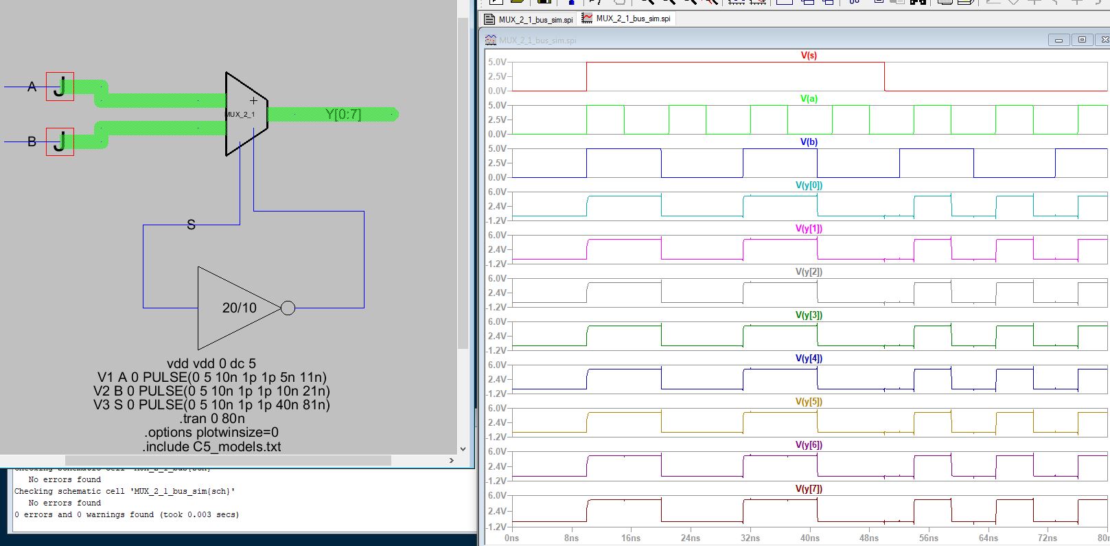 Figure 5. 8-bit AND gate schematic using buses.
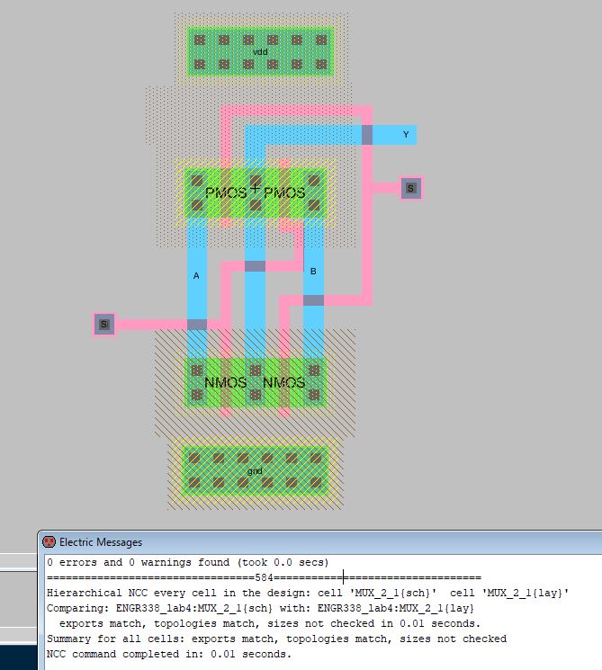
Figure 6. 2:1 mux layout
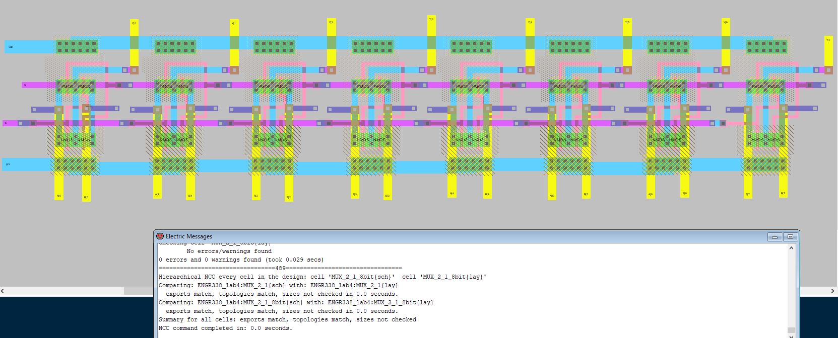
Figure 7. 8-bit mux layout
Task 2.
A
schematic and layout of a 1-bit high speed full adder were
created. DRC checks were run throughout
the process, and a simulation was run in LTSpice.
Figure 8. 1-bit high speed full adder schematic.
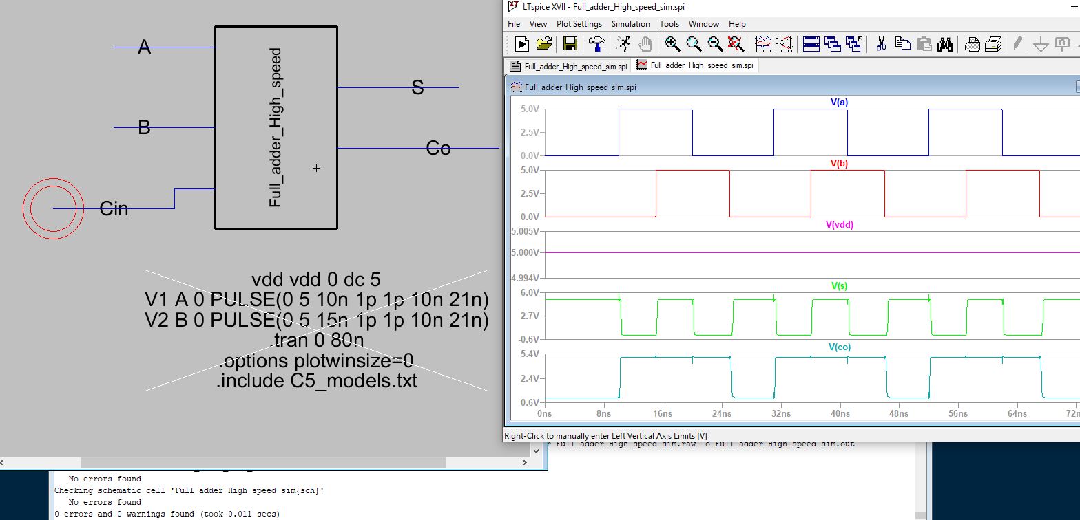
Figure 9. 1-bit high speed full adder simulation in LTSpice.
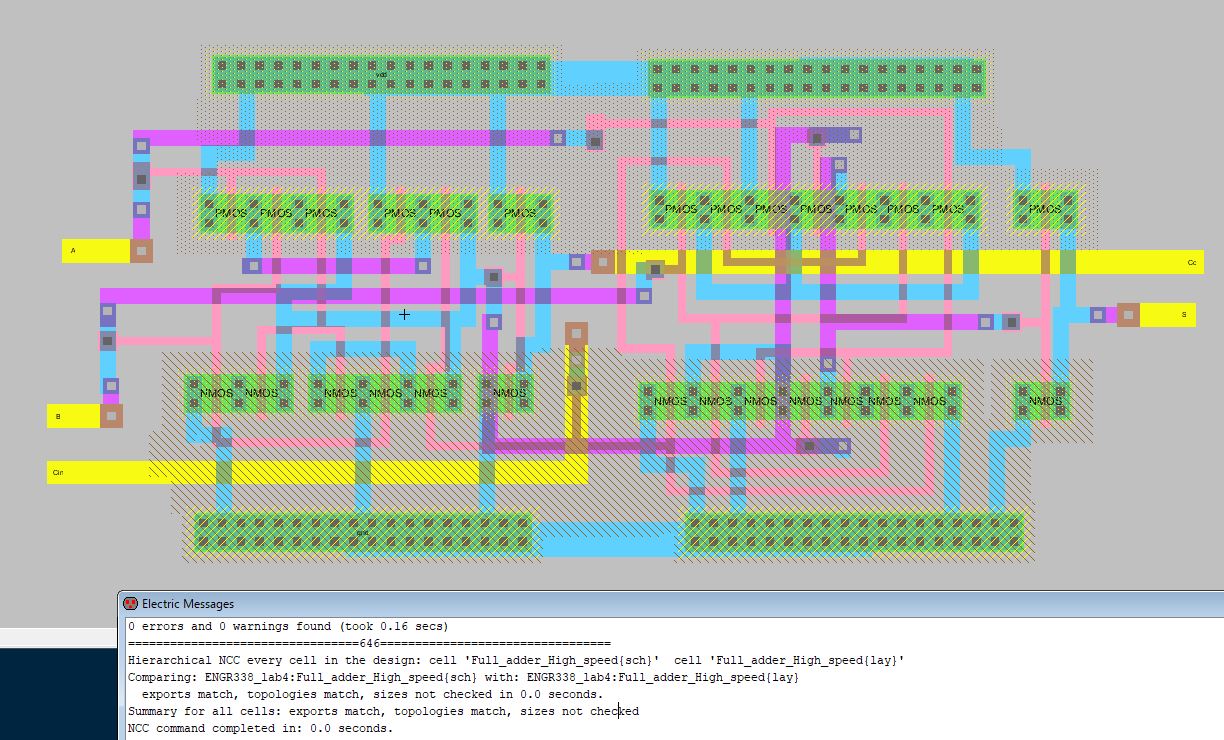
Figure 10. 1-bit high speed full adder layout.
Task 3.
The 8-bit high speed full adder
schematic was created by using buses and the 1-bit high speed full adder.
The layout was also created using 8 subcells. LTSpice was used to
simulate the logic. DRC checks were run throughout
the process.
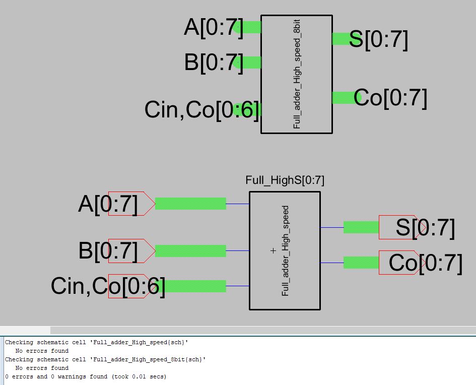
Figure 11. 8-bit high speed full adder schematic and icon using buses.
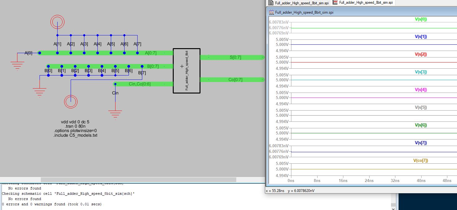
Figure 12. Simulating the logic of the 8-bit high speed full adder schematic using LTSpice.
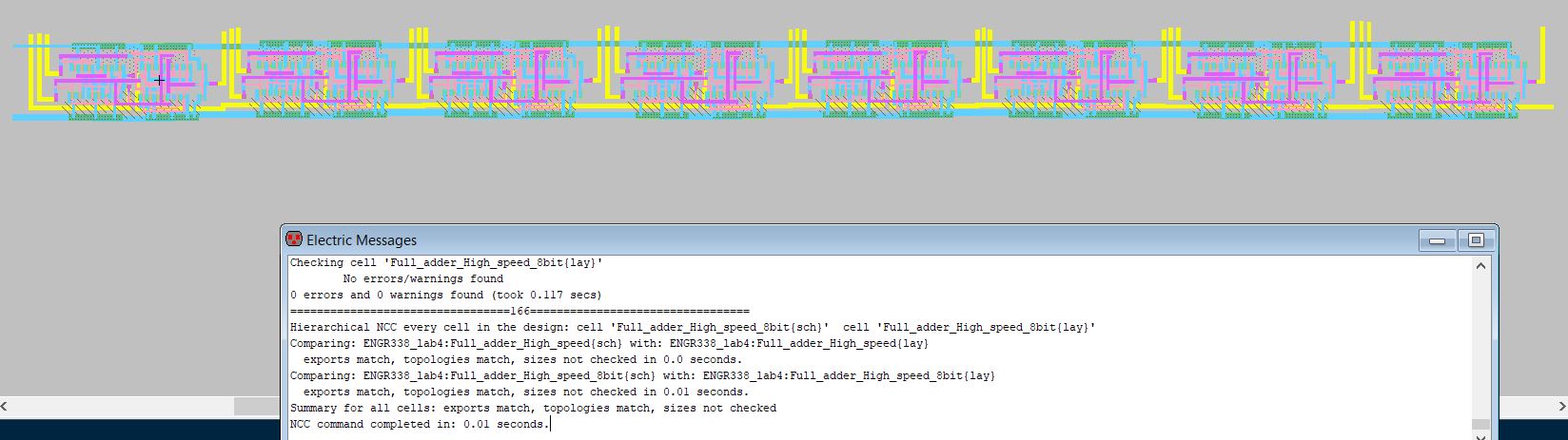
Figure 13. 8-bit high speed full adder layout.
2. Discussion
This
lab allowed me to gain more experience using ElectriVLSI. The lab was
implemented successfully. I was able to create the schematic and layout
for high speed full adders and muxes. I also gained gained more
experience using buses and arrays to create multi-bit gates.