ENGR338
2021 Spring
Lab 7: Using Buses in ElectriVLSI
Sophie Turner
sjturner@fortlewis.edu
Using Buses in ElectriVLSI
1. Introduction
The
purpose of this lab was to build a ring
oscillator using buses and building multi-bit gates in ElectriVLSI.
Previous built
1-bit AND, OR, NAND, and NOR gates were used to create 8-bit gates for
each
logic gate. The logic was verified using LTSpice for each 8-bit gate.
DRC and NCC checks were run throughout the process to ensure the
components were correct.
2. Methods
ElectriVLSI was used to create the designs for
8-bit AND, OR, NAND, and NOR gates as well as the ring oscillator. LTSpice was
used to simulate the ring oscillator and the four multi-bit logic gates were verified. For more detailed
methods go http://www.yilectronics.com/Courses/ENGR338L_CE/lab7_TheBus/Lab7.html
3. Results
Task 1.
A schematic and layout of a ring oscillator were
created. The inverter layout was edited to have the vdd and gnd rails be closer
together. The oscillator layout was created by combining 10 inverter_short
layouts together. A new schematic was created where eleven inverters were
connected in a loop to create a ring oscillator. DRC checks were run throughout
the process, and a simulation was run in LTSpice.
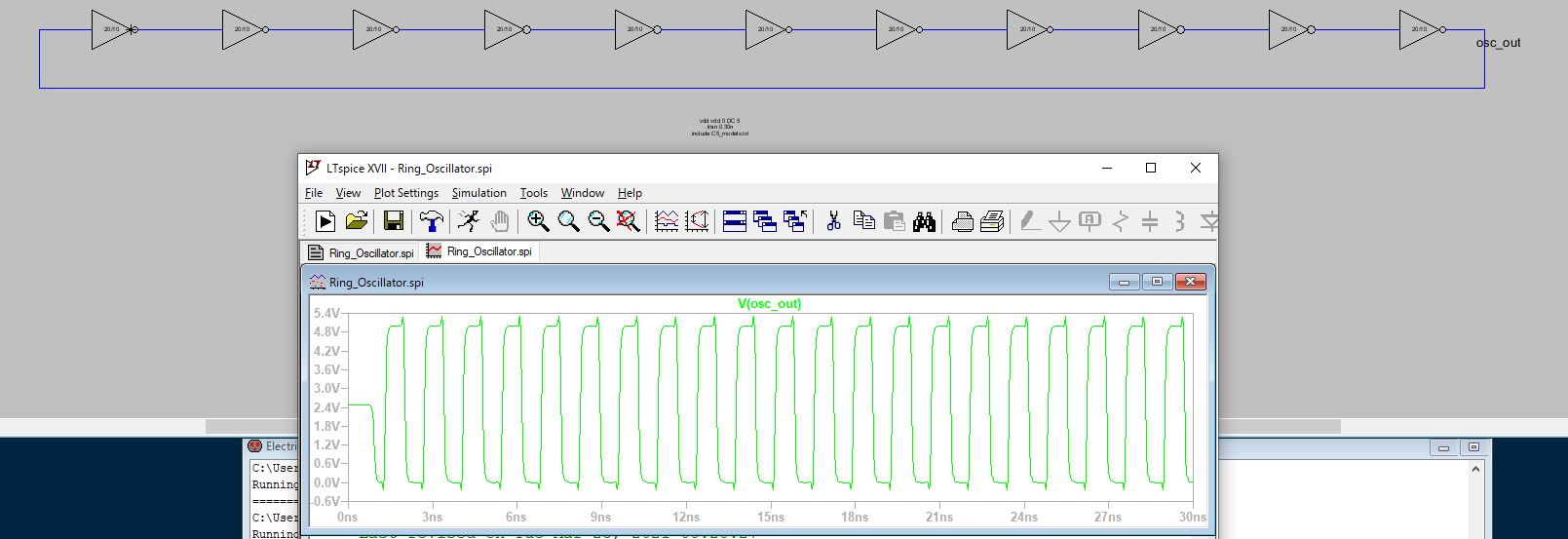
Figure 1. Ring oscillator schematic and LT Spice
simulations.
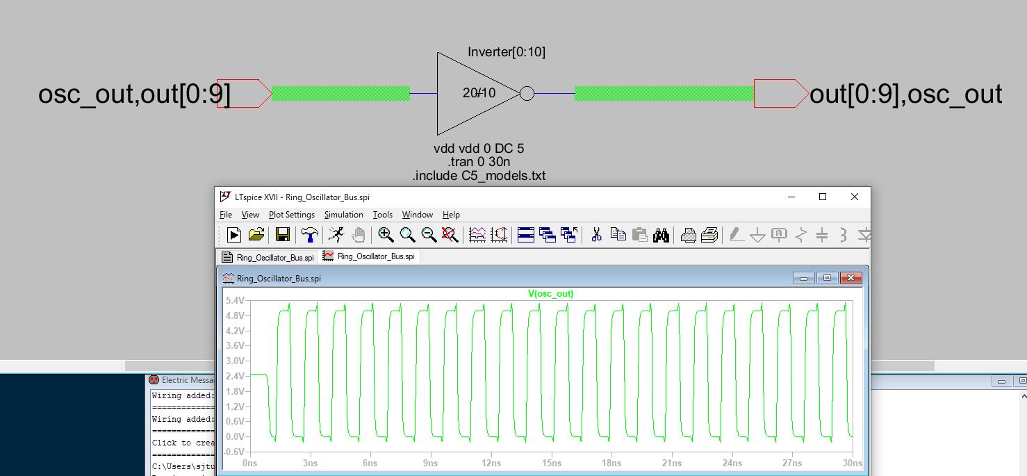
Figure 2. Ring oscillator schematic using buses.
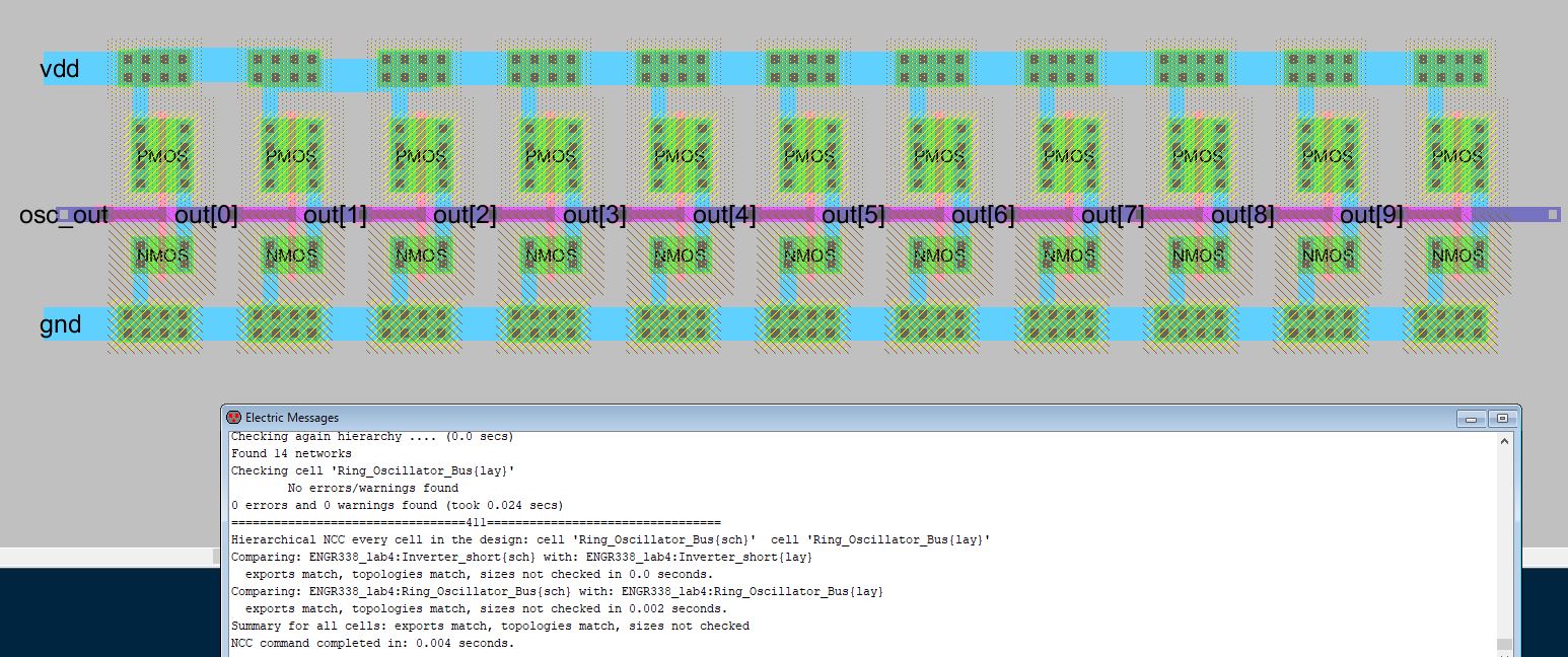
Figure 3. Ring oscillator layout using inverter_short.
Task 2.
An
8-bit AND gate was designed using the AND gate created in a previous lab and by
using buses. The schematic was simulated in LTSpice to verify the
logic. A layout was also created using 8 of the previously made AND layouts to create the multi-bit gate. DRC and NCC checks were run throughout the process.
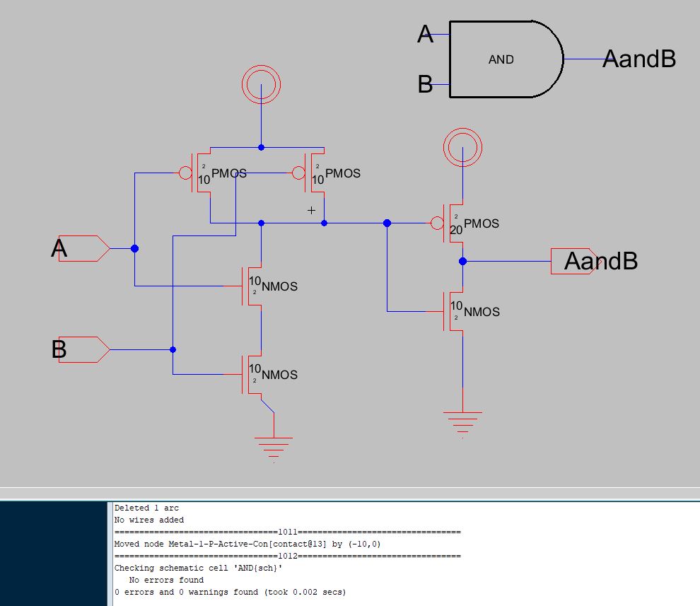
Figure 4. Checking the AND schematic for errors.
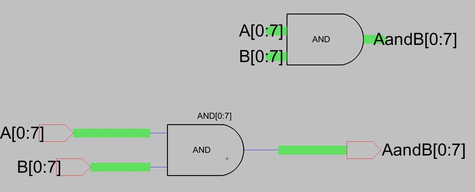
Figure 5. 8-bit AND gate schematic using buses.
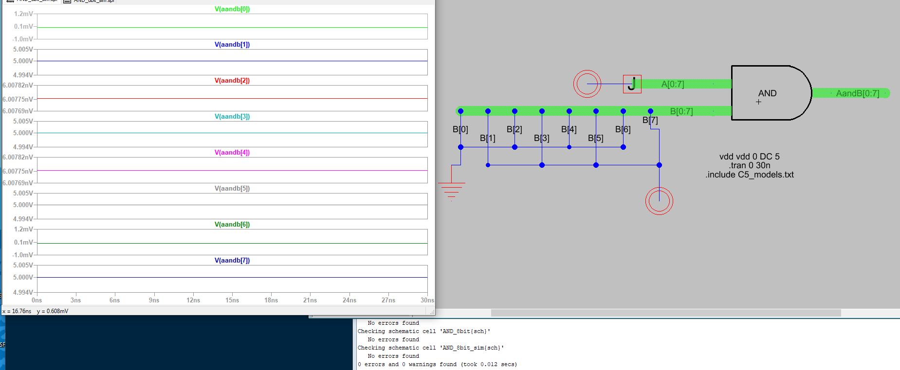
Figure 6. Connecting the A[0:7] gate to vdd and simulating
the logic using LTSpice.
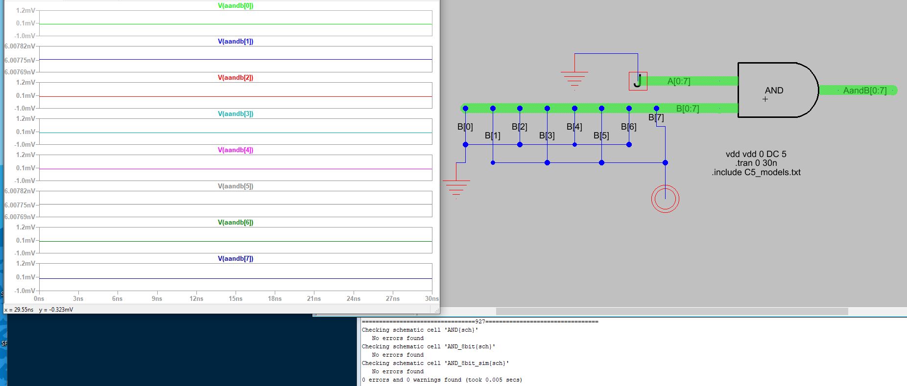
Figure 7. Connecting the A[0:7] gate to gnd and simulating
the logic using LTSpice.
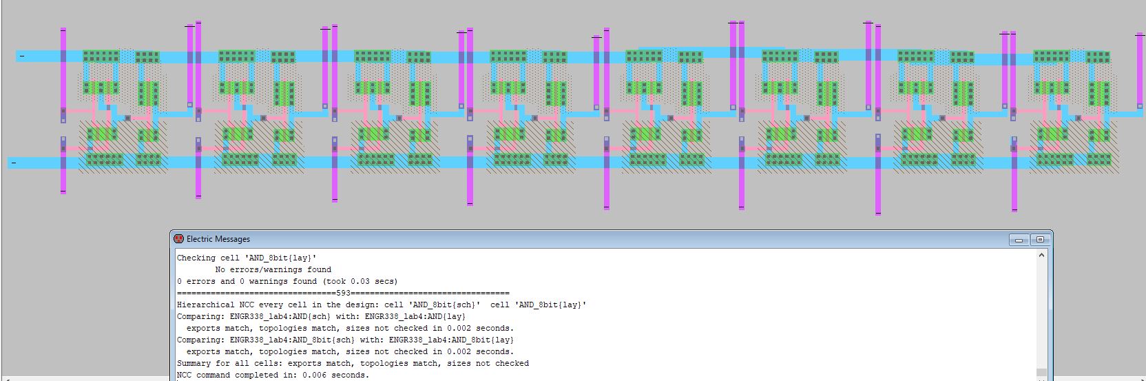
Figure 8. 8-bit AND gate layout.
Task 3.
An 8-bit OR gate was designed using the OR gate created in a previous lab and buses. The schematic was simulated in LTSpice to verify the
logic. A layout was also created using 8 of the previously made OR layouts to create the multi-bit gate. DRC
and NCC checks were run throughout the process.
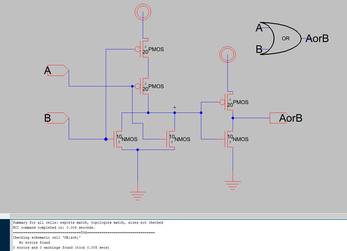
Figure 9. Checking the OR gate schematic for errors.
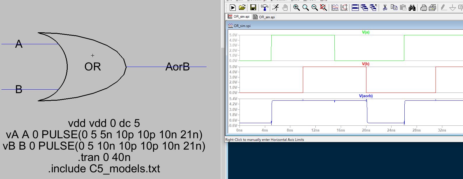
Figure 10. OR schematic and verifying the logic using LTSpice.
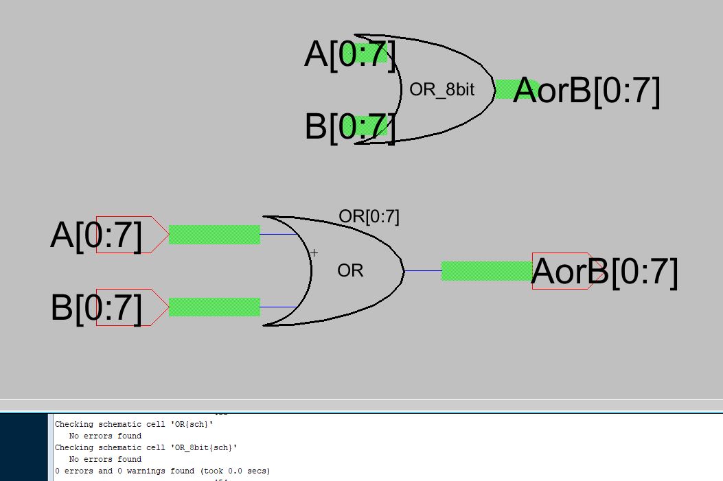
Figure 11. 8-bit OR schematic and icon using buses.
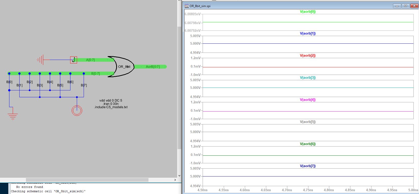
Figure 12. Simulating the logic of the 8-bit OR schematic using LTSpice.
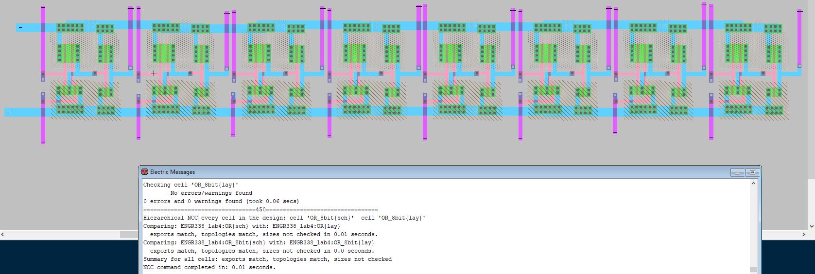
Figure 13. 8-bit OR gate layout.
Task 4.
An 8-bit NAND gate was designed using the previously made NAND gate and buses.
A layout was also created using 8 of the previously made NAND layouts
to create the multi-bit gate. The NAND logic was simulated and verified
using LTSpice. DRC
and NCC checks were run throughout the process.
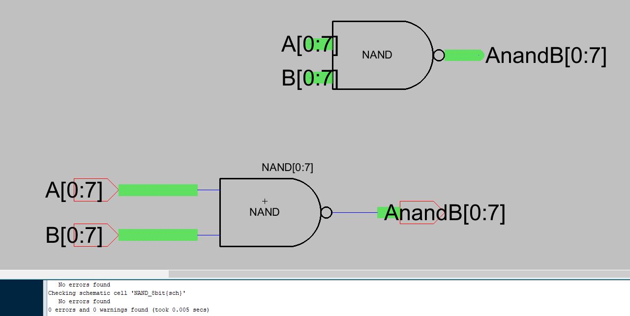
Figure 14. 8-bit NAND schematic and icon using buses.
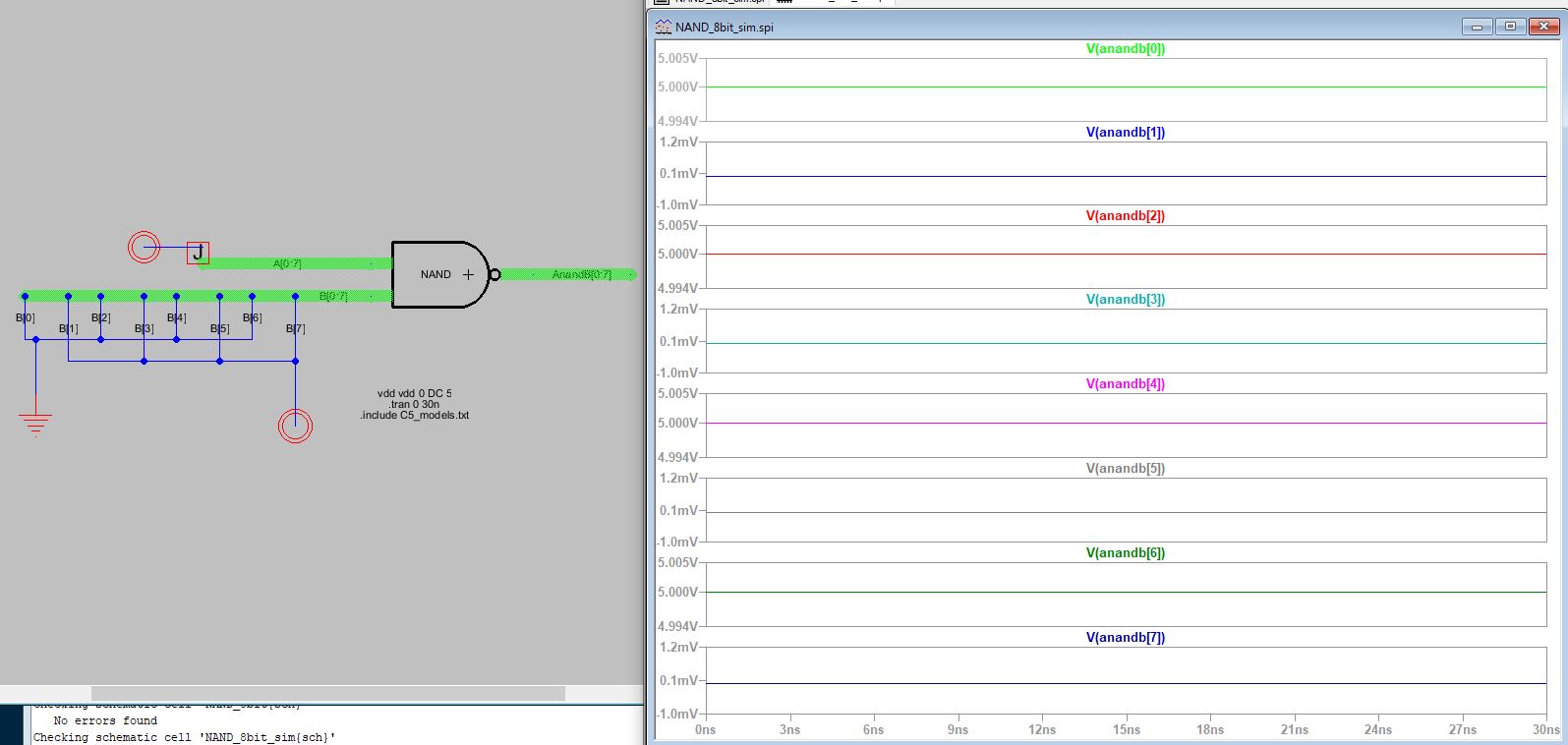
Figure 15. Simulating the logic of the 8-bit NAND schematic using LTSpice.
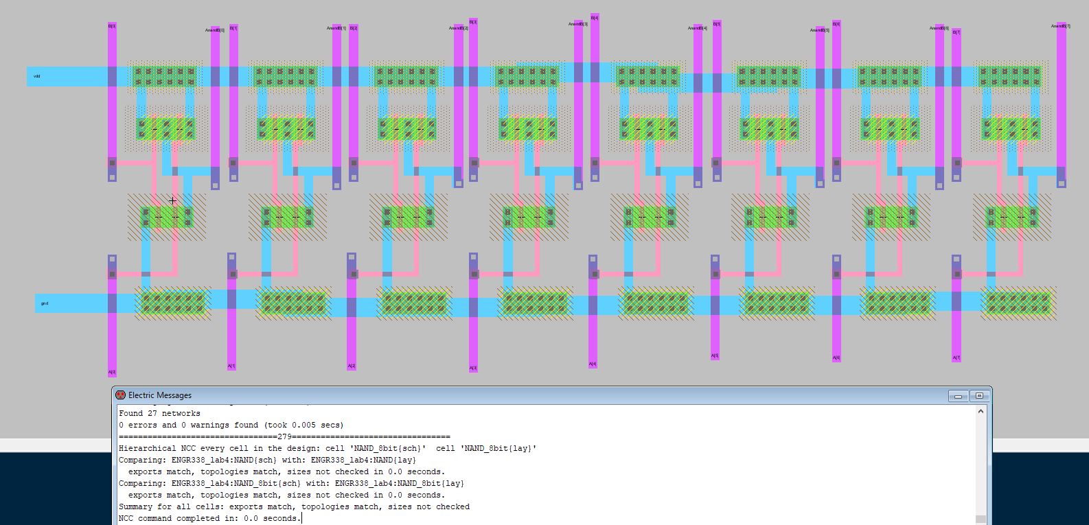
Figure 16. 8-bit NAND gate layout.
Task 5.
An 8-bit NOR gate was designed using the previously made NOR gate and buses. A layout was also created using 8 of the previously made NOR layouts to create the multi-bit gate. The NOR logic was simulated and verified using LTSpice. DRC
and NCC checks were run throughout the process.
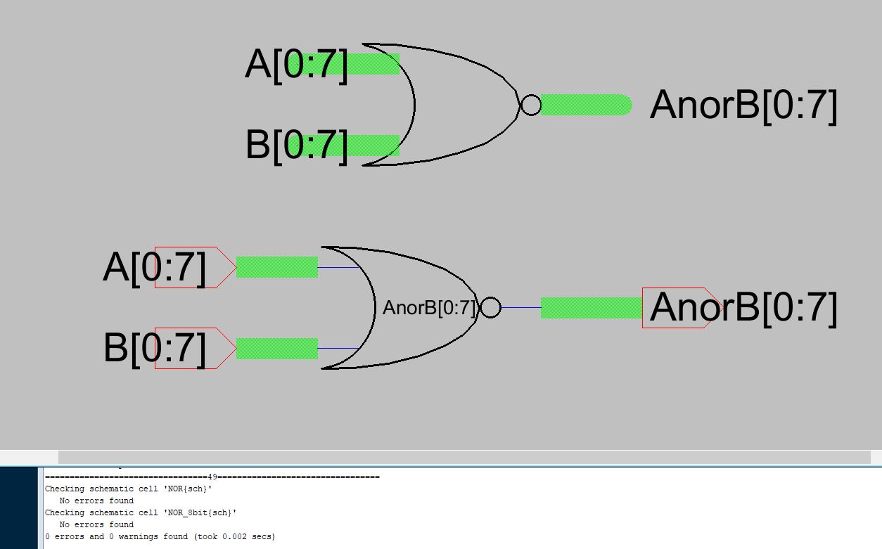
Figure 17. 8-bit NOR schematic and icon using buses.
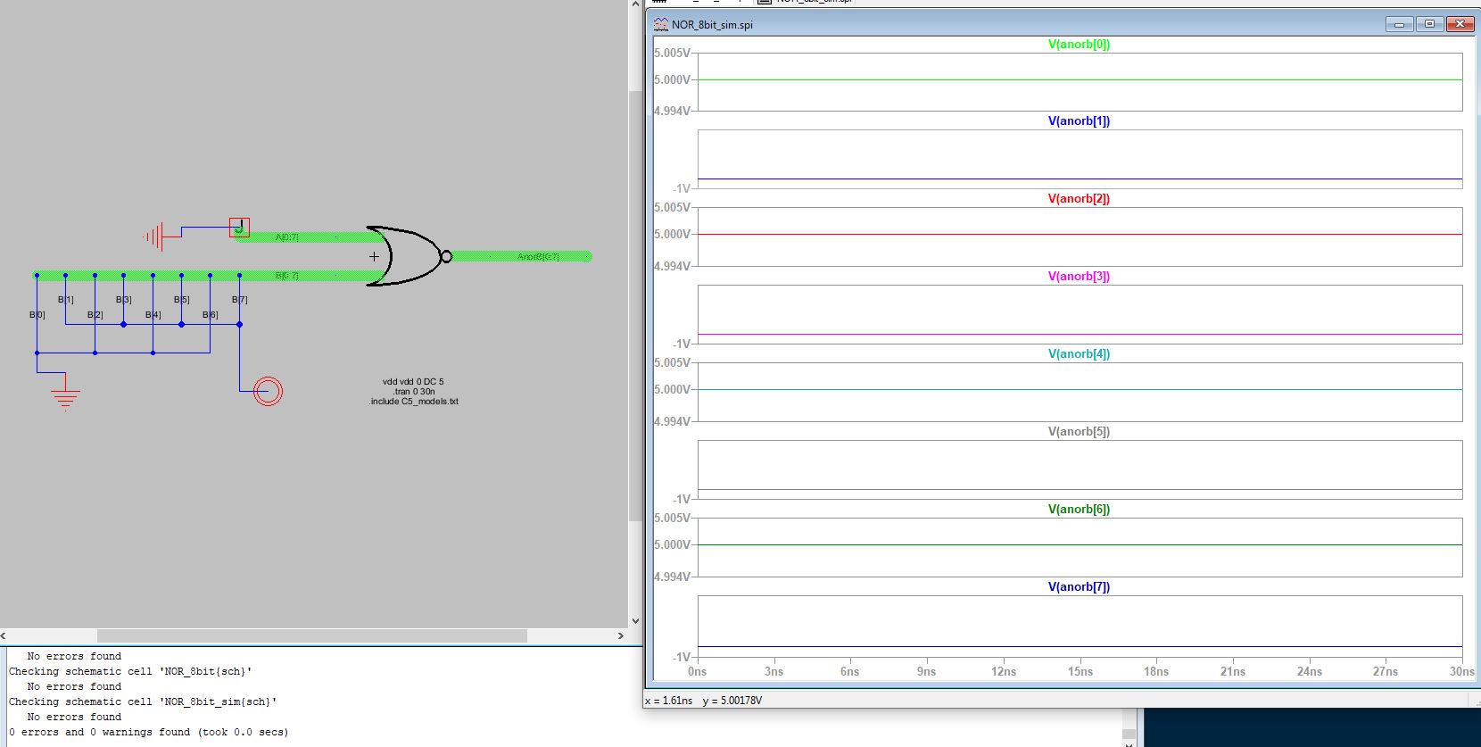
Figure 18. Simulating the logic of the 8-bit NOR schematic using LTSpice.
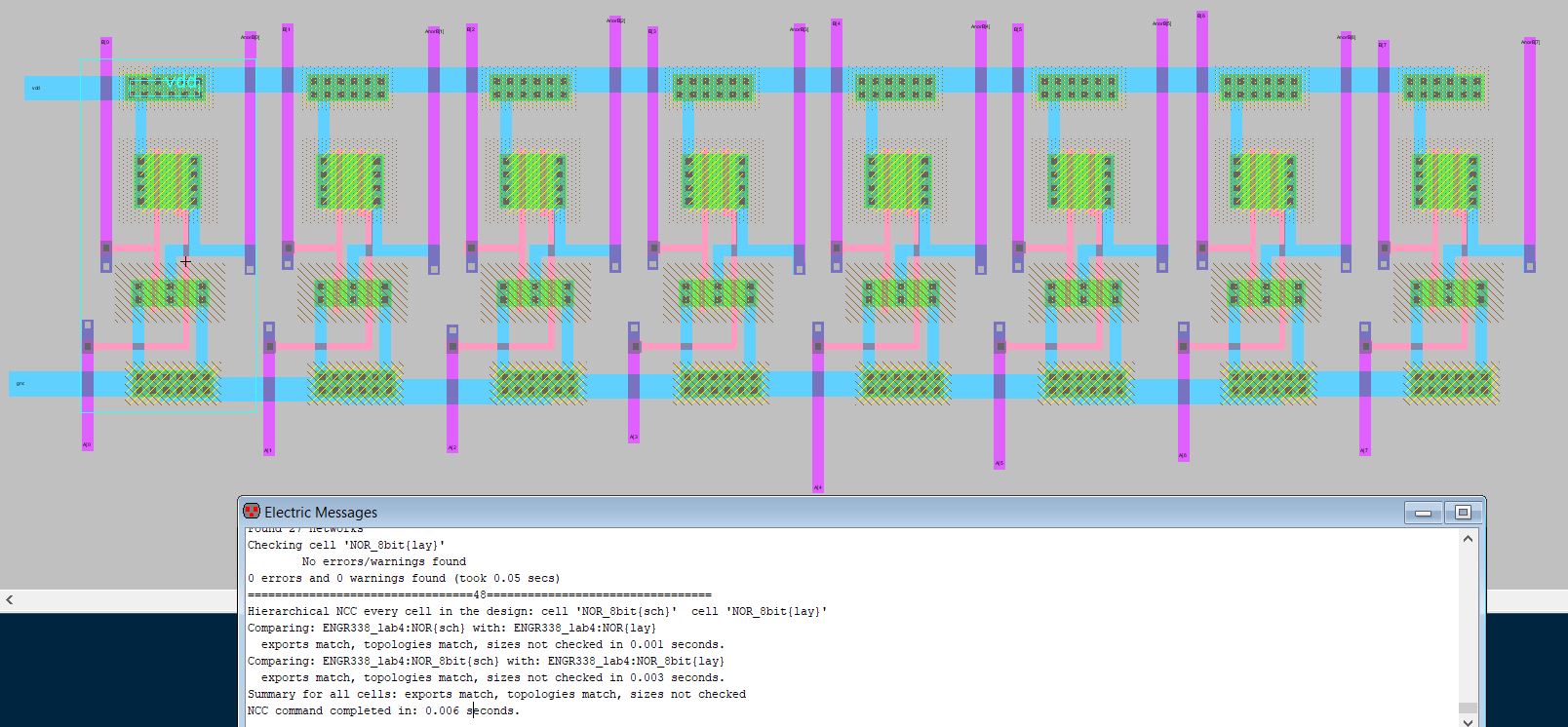
Figure 19. 8-bit NOR gate layout.
2. Discussion
This
lab allowed me to gain more experience using ElectriVLSI. The lab was
implemented successfully. I was able to create the schematic and layout
for multi-bit gates. I also gained experience using buses and arrays to create multi-bit gates.