ENGR338
2021 Spring
Lab 6: Build a NAND, NOR, XOR, and Full Adder
Sophie Turner
sjturner@fortlewis.edu
Build a NAND, NOR, XOR, and Full Adder
1. Introduction
The purpose of this lab was to create a NAND,
NOR, XOR, and Full adder in ElectriVLSI. The schematic, icon, and layout were
created for the three logic gates and the full adder. PMOS and NMOS transistors
were used to create the layouts and schematics. LTSpice was used to simulate
each icon to verify its functionality. By combining the logic gates created,
the Full adder was created. DRC and NCC checks were run throughout the process
to ensure the components were correct.
2. Methods
ElectriVLSI was used to create the design a
NAND, NOR, XOR, and Full adder. LTSpice was used to simulate the schematics.
For more detailed methods go to http://yilectronics.com/Courses/ENGR338L_CE/lab6_NAND_NOR_XOR_FA/Lab6.html.
3. Results
Task 1.
A schematic and layout of the NAND gate were
created. An icon was edited to be a NAND gate shape as seen in Figure 1. DRC
checks were run, and a simulation of the NAND gate was run in LTSpice. A layout
was also created for the NAND gate as seen in Figure 3. The PMOSes were in
parallel and the NMOSes were in series as seen in Figure 3. Wires were
connected and a NCC and DRC checks were run on the layout.
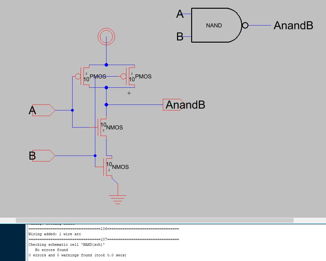
Figure 1. Created an icon and schematic of a NAND gate using NMOS and PMOS transistors.
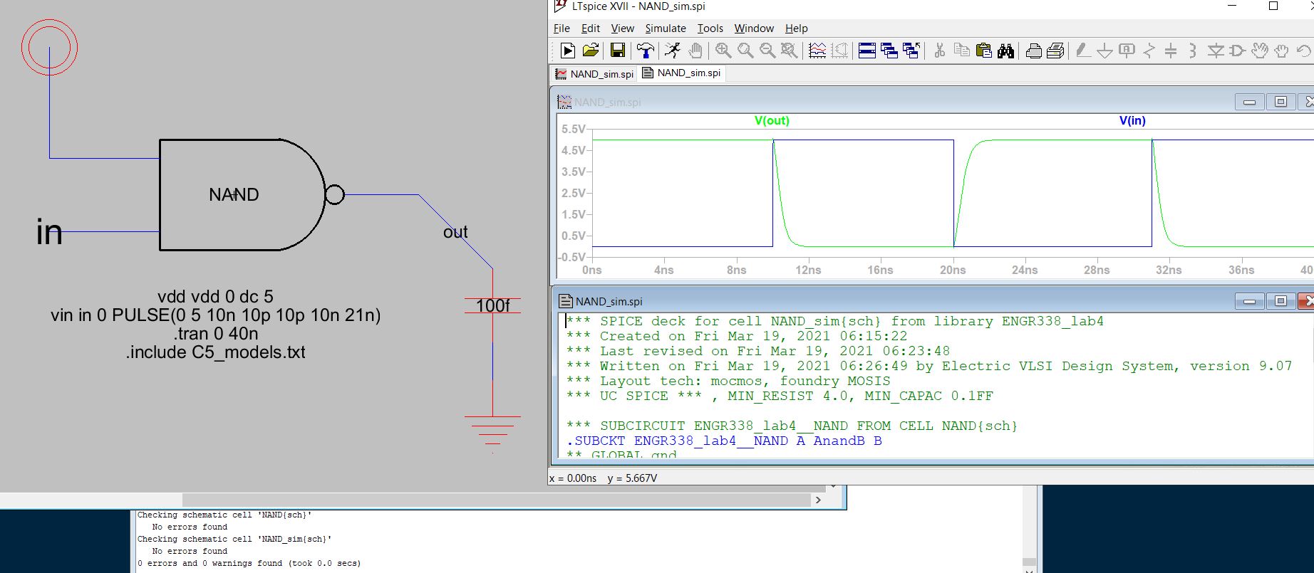
Figure 2. NAND gate simulation with LTSpice.
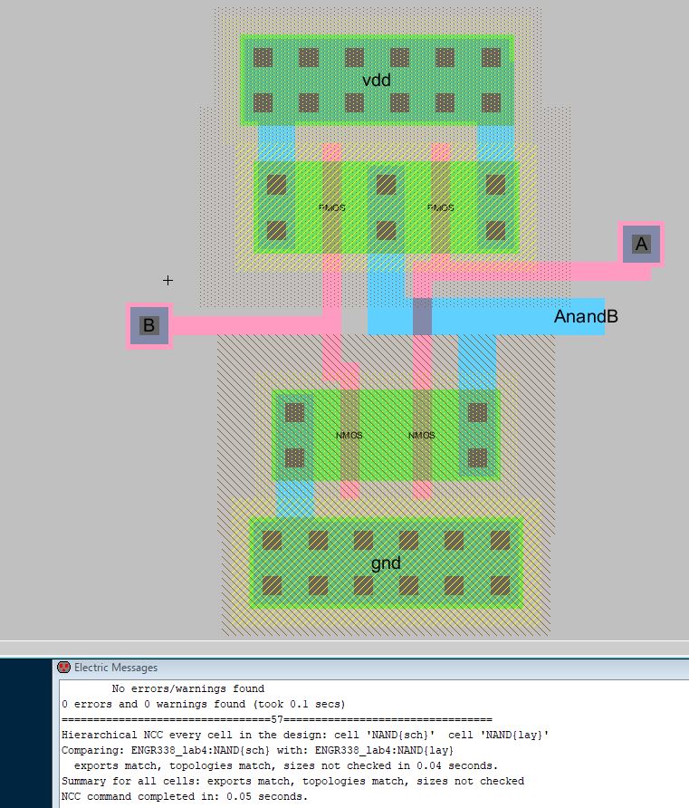
Figure 3. NAND gate layout.
Task 2.
A
schematic and layout of the NOR gate were created. A icon was
edited to be a NOR gate shape as seen in Figure 4. DRC checks were run
and a simulation of the NOR gate was run in LTSpice. A layout was also
created for the NOR as seen in Figure 6. The PMOSes were in series and
the NMOSes were in parallel as seen in Figure 6. Wires were
connected and a NCC and DRC checks were run on the layout.
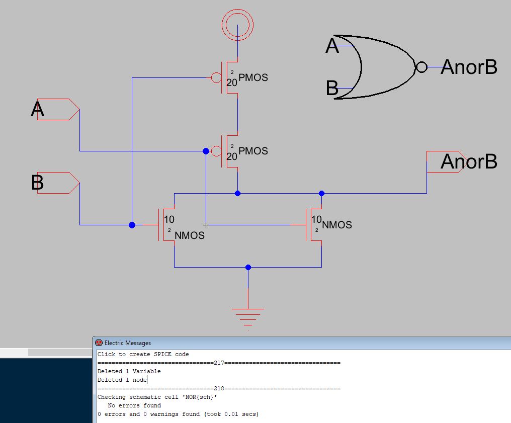
Figure 4. Created an icon and schematic of a NOR gate using NMOS and PMOS transistors.
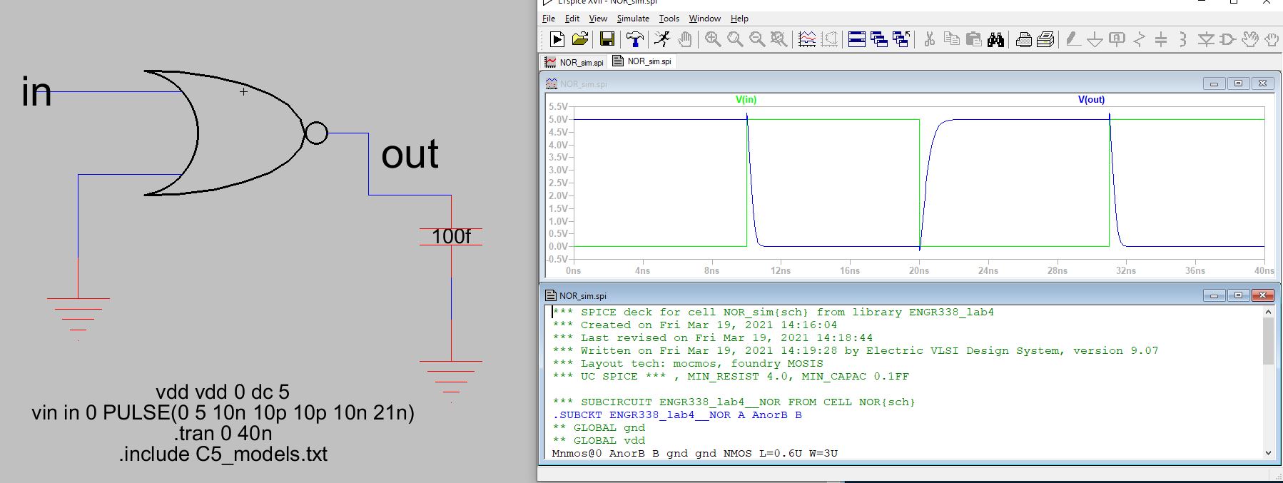 Figure 5. NOR gate simulation with LTSpice.
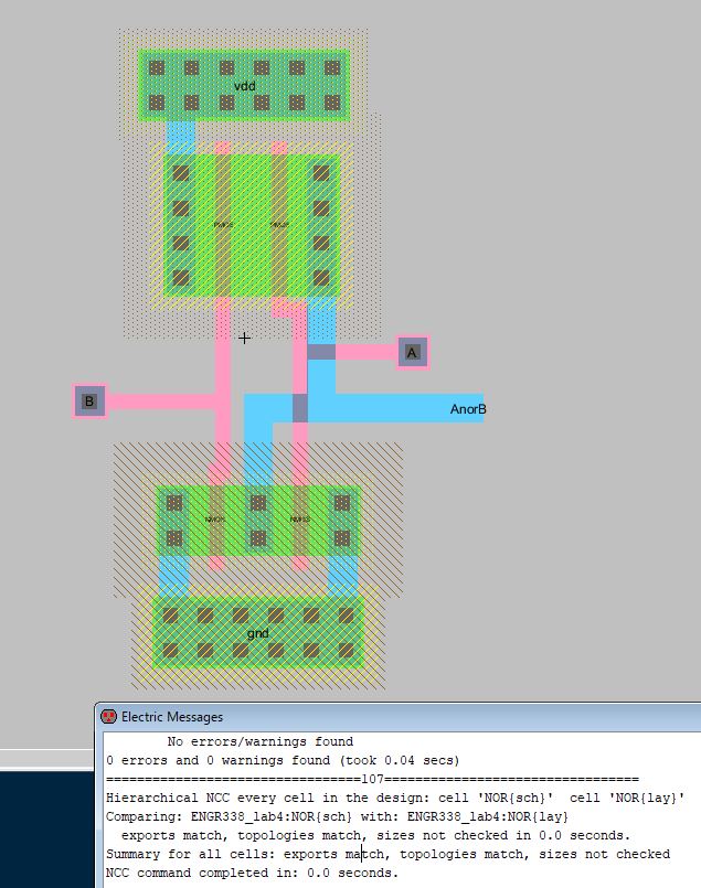
Figure 6. NOR gate layout.
Task 3.
A schematic and layout of the XOR gate were
created. A icon was also edited to be a XOR gate shape as seen in Figure 7. DRC
checks were run and a simulation of the XOR gate was run in LTSpice. A layout
was also created for the XOR gate as seen in Figure 9. DRC checks were
constantly checked to ensure the layout was correct and a final NCC check was
performed to make sure the schematic and layout matched.
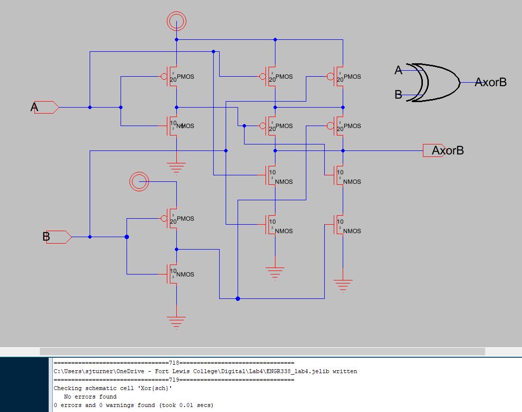
Figure 7. Created an icon and schematic of a XOR gate using NMOS and PMOS transistors.
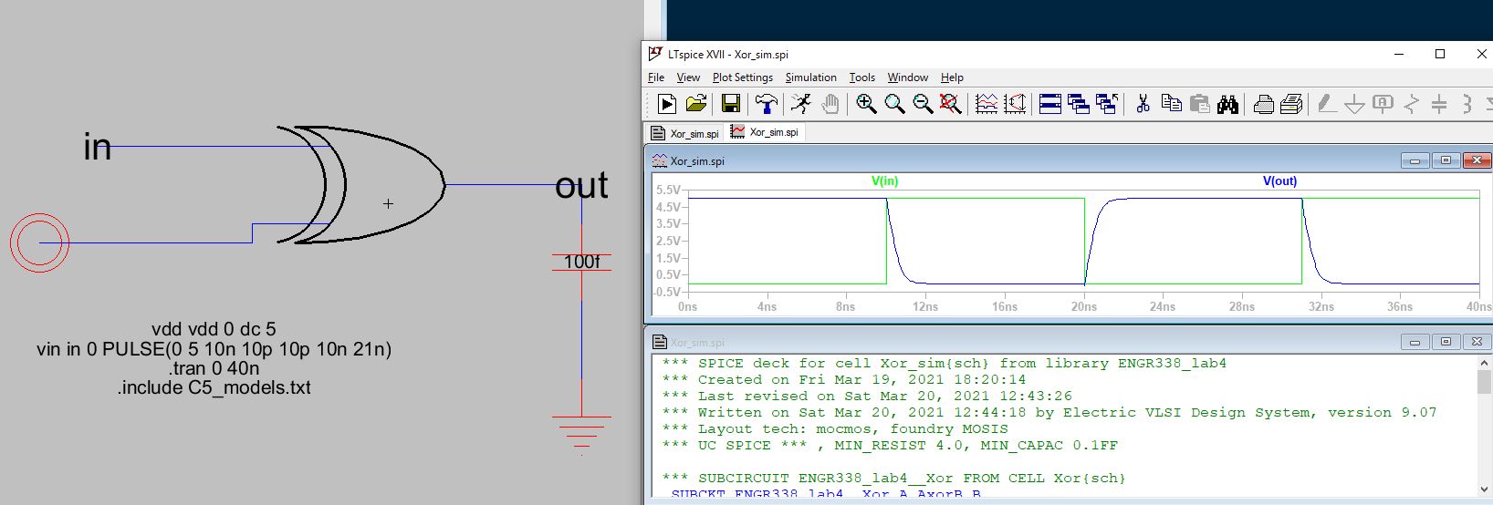
Figure 8. XOR gate simulation with LTSpice.

Figure 9. XOR gate layout.
Task 4.
A schematic and layout, and icon were created
for the Full adder. The XOR, NAND, inverter, and NOR gates created previously
were combined to create the Full adder. For the layout the layouts of the logic
gates were combined using Metal1-Metal2 vias. DRC checks were run constantly
and a final NCC check was also performed. Two simulations were run in LTSpice.
When Cin was connected to vdd there was more noise within the simulation, and
the V(cout) was inverted compared to when Cin was connected to gnd as seen in
Figures 11 and 12.
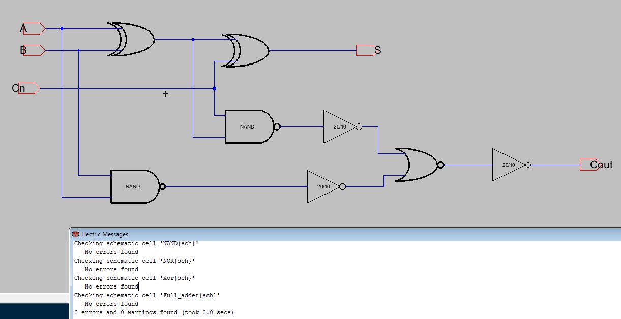
Figure 10. Schematic for the Full adder using the NAND, NOR, XOR, and inverter icons.
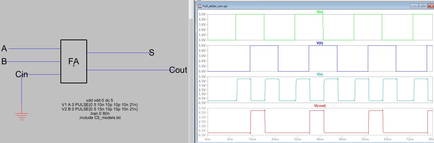
Figure 11. Simulation of the Full adder when Cin is connected to gnd.
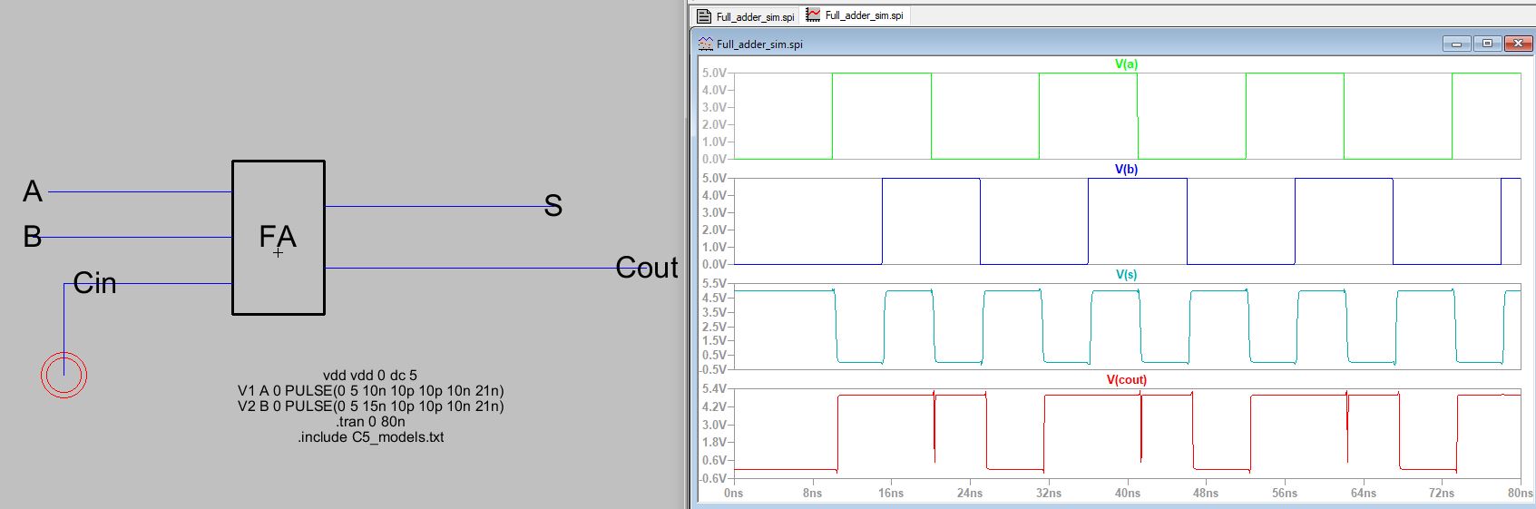
Figure 12. Simulation of the Full adder when Cin is connected to vdd.
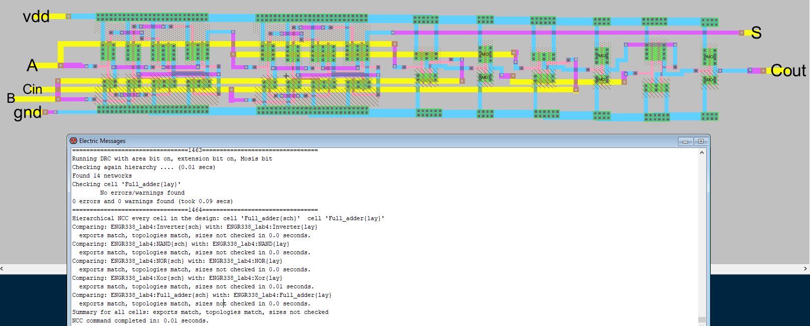
Figure 13. Full adder layout.
2. Discussion
This
lab allowed me to gain more experience using ElectriVLSI. The lab was
implemented successfully. I was able to create the schematic, icon, and layout
for the Full adder, NOR, NAND, and XOR logic gates and simulate their functionality
using LTSpice. This lab took patients, persistence and a lot of DRC checks to successfully
complete. I gained experience using ElectriVLSI to create a combinational circuit.