ENGR338
2021 Spring
Lab 5: The Inverter
Sophie Turner
sjturner@fortlewis.edu
The Inverter
1. Introduction
The
purpose of this lab was to simulate an inverter in ElectriVLSI. An
inverter schematic using PMOS and NMOS transistor was created, as well
as the icon and layout. LTSpice, IRSIM, and ALS simulation tools were
used to simulate the inverters.
2. Methods
ElectriVLSI
was sued to create the design of an inverter. LTSpice and IRSIM were
used to simulate the inverters. For more detailed methods go to http://yilectronics.com/Courses/ENGR338L_CE/lab5_Inverter/Lab5.html .
3. Results
Task 1.
A schematic of an inverter was created using a 20/2 PMOS
transistor and a 10/2 NMOS. An icon was created and simulated using
LTSpice. A new simulation was also run on LTSpice using PULSE input as
seen in Figure 3.
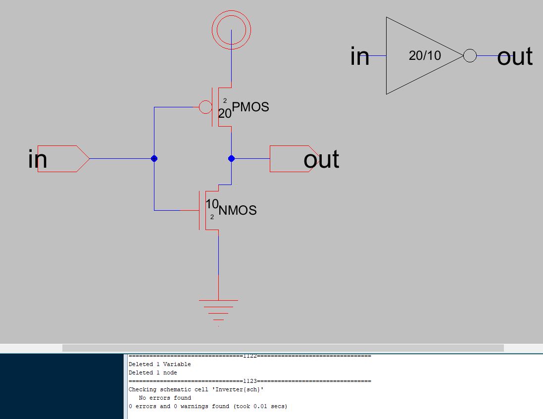
Figure 1. Creating a schematic of a inverter using NMOS and PMOS transistors.
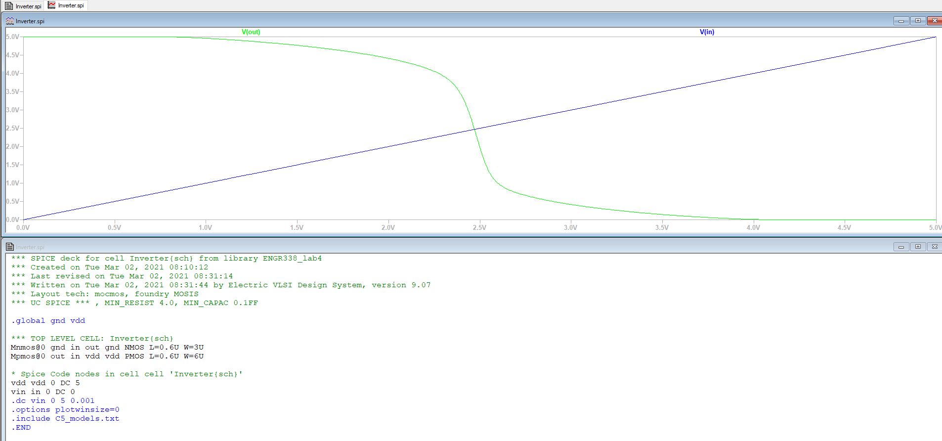
Figure 2. Inverter simulation with LTSpice.
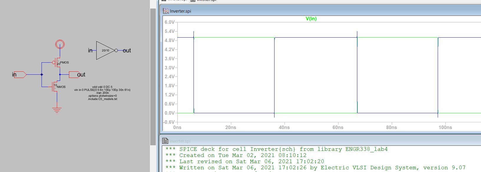
Figure 3. LTSpice simulation of the inverter using a PULSE input.
Task 2.
The layout for the 20/2 and 10/2 inverter was created and DRC and NCC error checks were run.
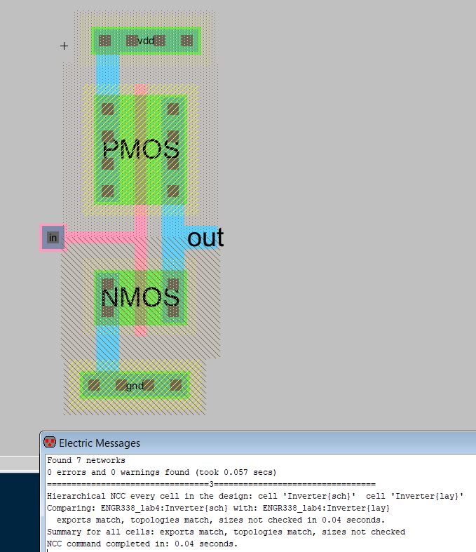
Figure 4. Layout for a 20/2 and 10/2 inverter.
Task 3.
A
schematic of an inverter was created using a 100/2 PMOS transistor and
a 50/2 NMOS. An icon was created and simulated using LTSpice. The
layout view was created and the DRC and NCC checks were run.
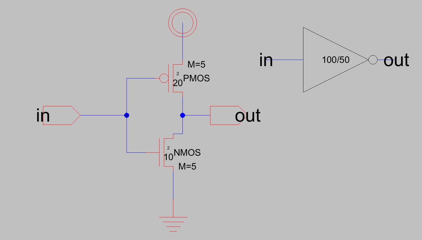
Figure 5. 100/2 and 50/2 inverter schematic and icon.
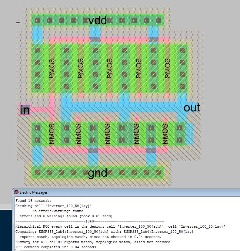
Figure 6. 100/2 and 50/2 inverter layout.
Task 4.
Simulations were run in LTSpice to verify the driving capability of the
two inverters. 100fF, 1pF, and 10pF capacitors were connected to the
inverters as seen in the figures below and the wavforms were simulated.

Figure 7. Simulation of the 20/10 inverter with a 100fF capacitor load.
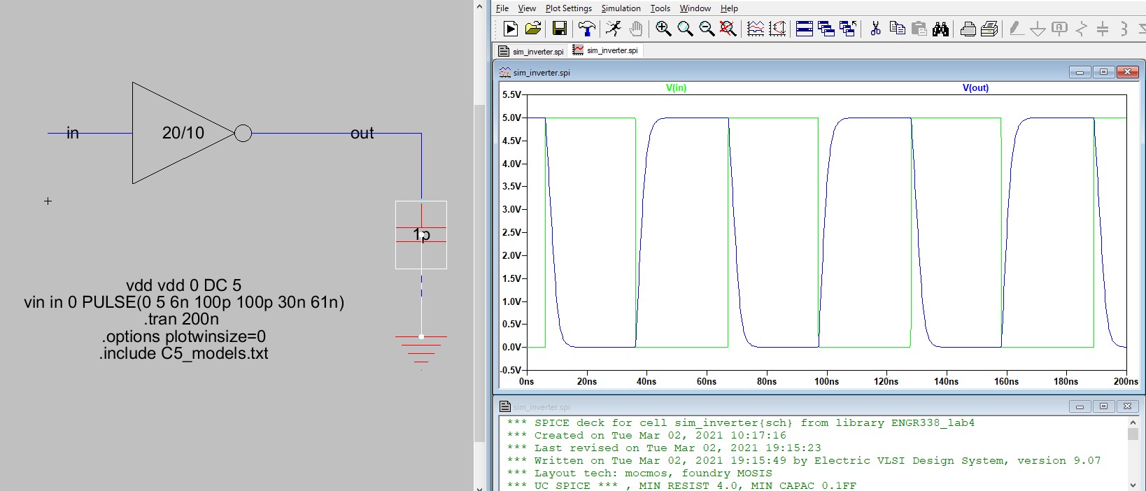
Figure 8. Simulation of the 20/10 inverter with a 1pF capacitor load.

Figure 9. Simulation of the 20/10 inverter with a 10pF capacitor load.
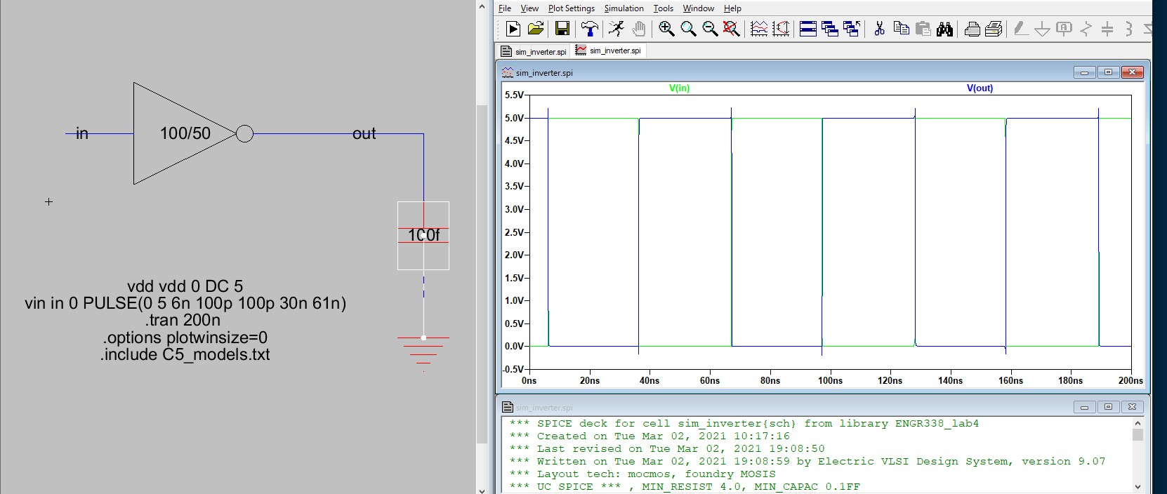
Figure 10. Simulation of the 20/10 inverter with a 10pF capacitor load.
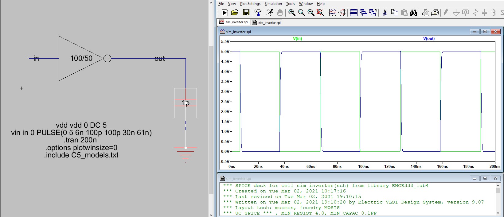
Figure 11. Simulation of the 100/50 inverter with a 1pF capacitor load.
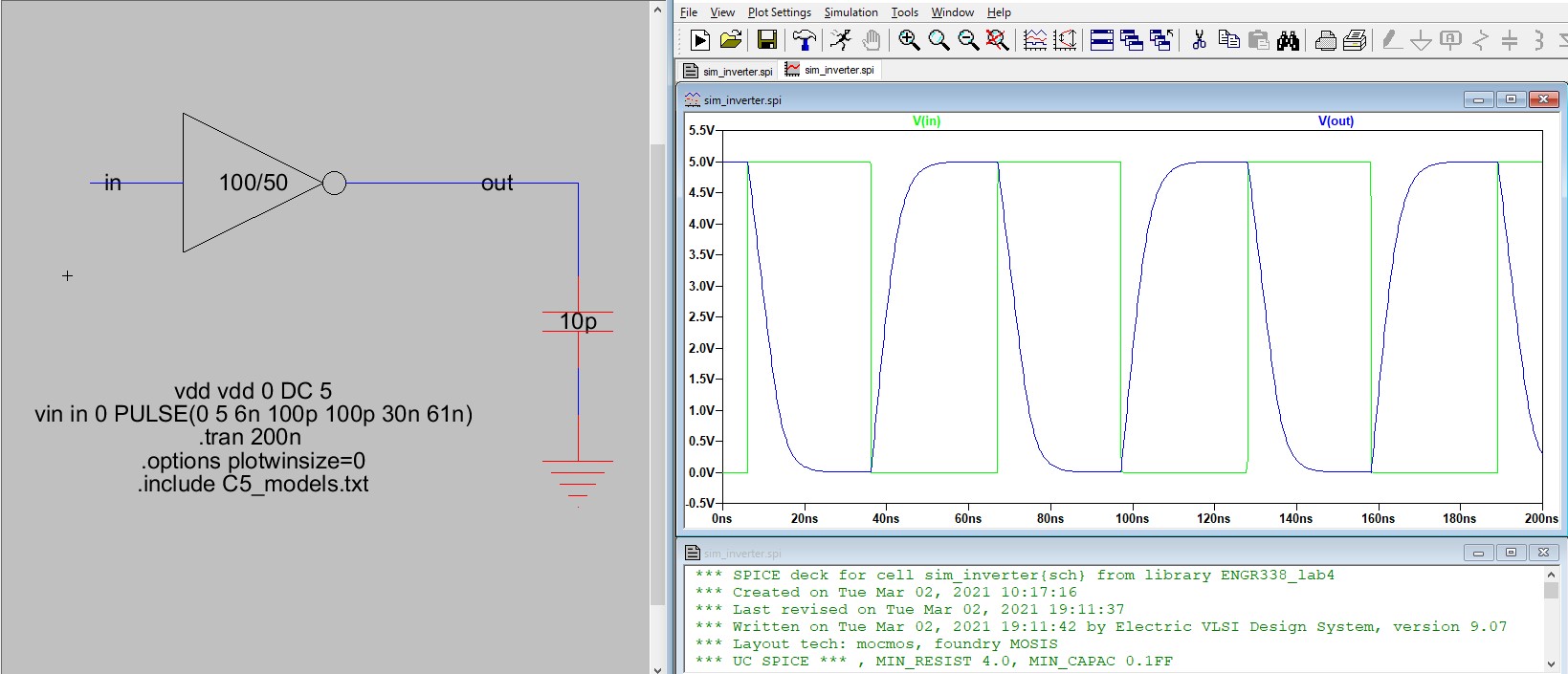
Figure 12. Simulation of the 100/50 inverter with a 10pF capacitor load.
Task 5.
The two inverters were connected and had a 100fF load added. The simulation of the schematic was simulated using ALS.
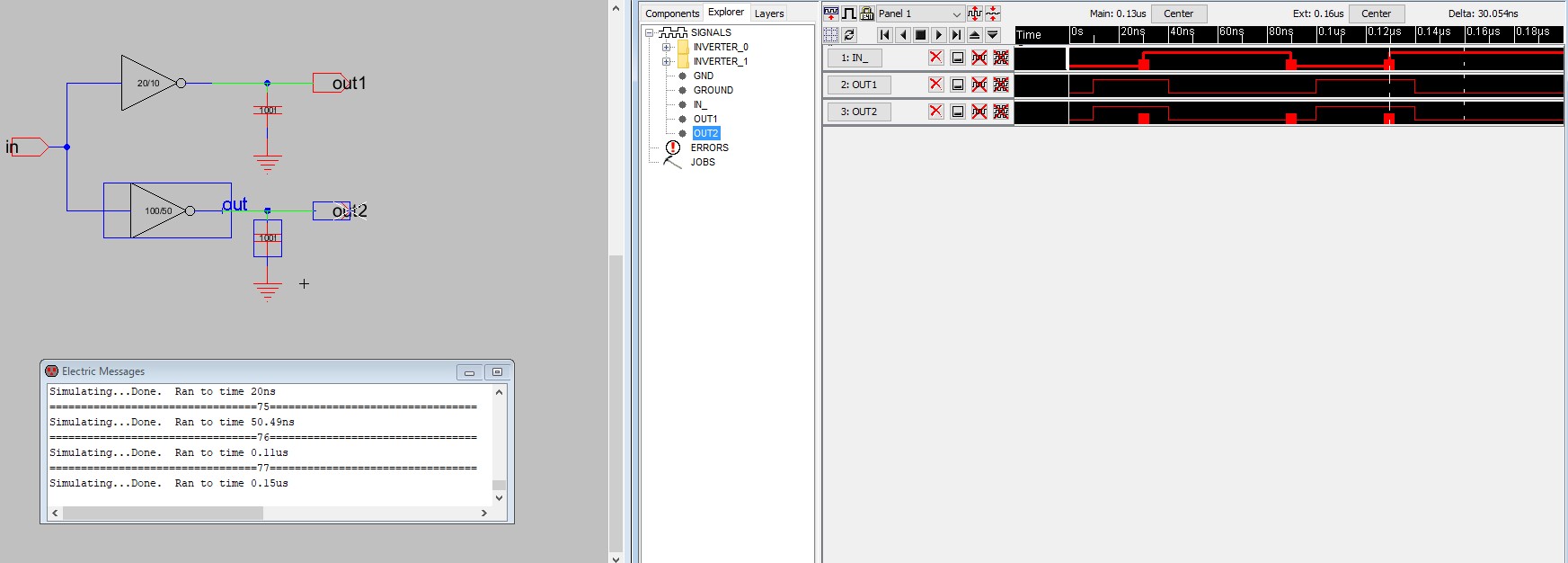
Figure 13. ALS simulation
The schematic in Figure 13 was also simulated using IRSIM.
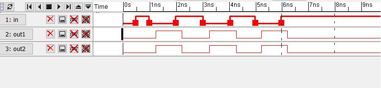
Figure 14. IRSIM simulation
2. Discussion
This
lab allowed me gain more experience using ElectriVLSI. The lab was
implemented sucessfully. I was able to create the schematic, icon, and
layout of a inverter and simulate their functionallity using LTSpice,
ALS and IRIM.