ENGR338
2021 Spring
Lab 2: Design an R-2R DAC
Sophie Turner
sjturner@fortlewis.edu
Design an R-2R DAC
1. Introduction
The purpose of this lab is to use ElectriVLSI
to design a R-2R digital to analog converter. LTSpice was used to
verify the DAC.
Task 1:
An ideal ADC/DAC (sim_ADC_DAC{schem}) file was copied to a new library and simulated using LTSpice as seen in Figure 2.
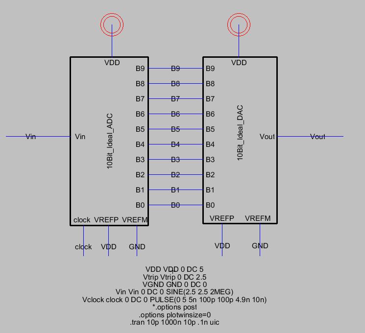
Figure 1. Existing ideal
ADC-DAC
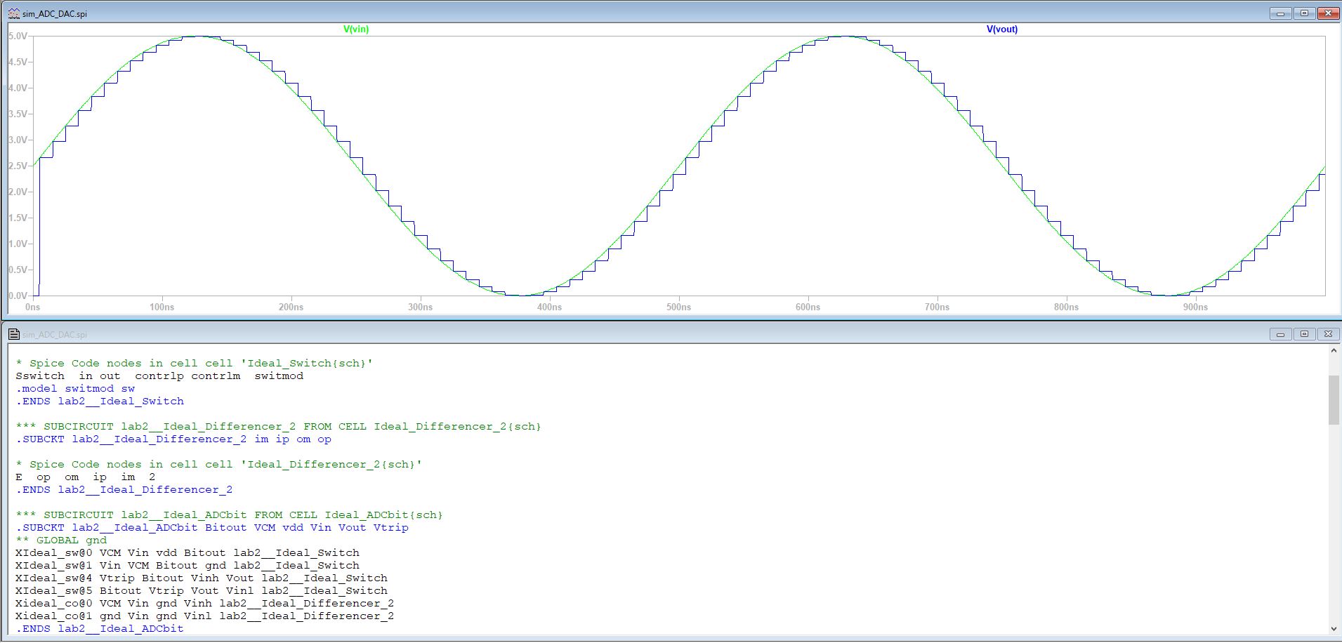
Figure 2. Existing ideal
ADC-DAC code and simulation.
Task 2
A R-2R ladder was built using n-well resistors,
pins and a GND component. An icon for the R-2R ladder was created and adjusted
to the given requirements. The R-2R ladder was connected to the 10-bit ideal
ADC.
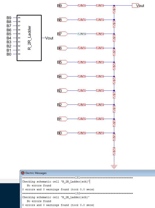
Figure
3. R-2R ladder schematic and icon.
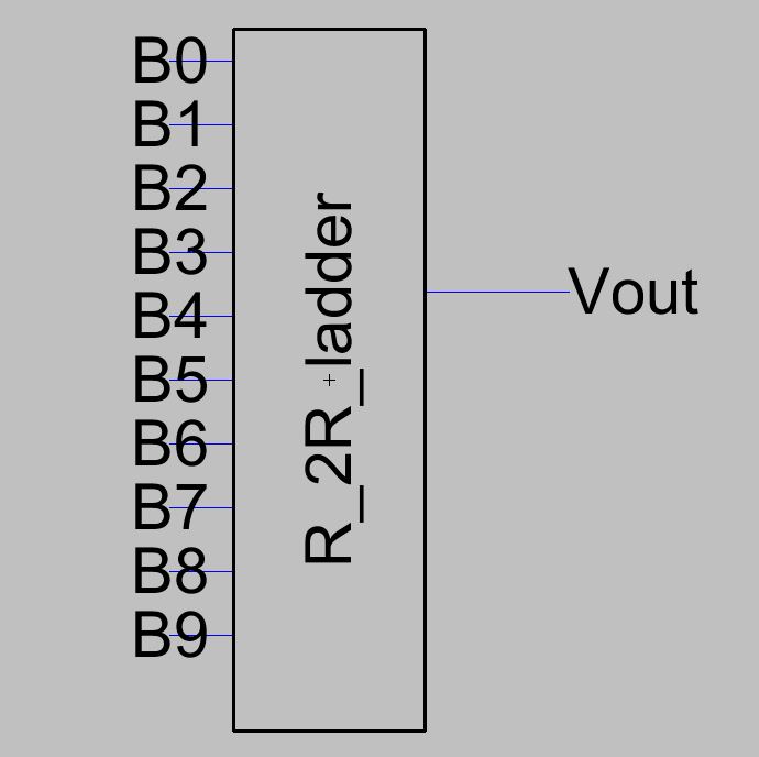
Figure 4. R-2R ladder icon
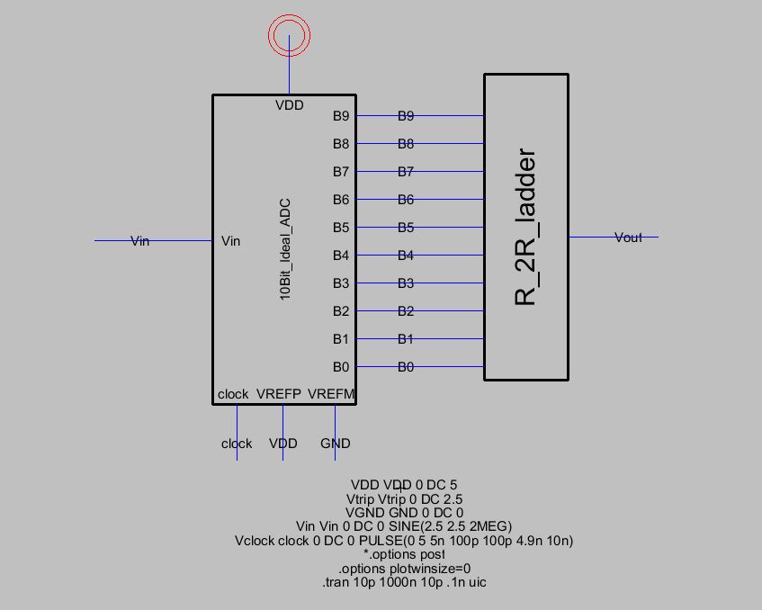
Figure 5. Existing ideal
ADC-DAC code and simulation.
LTSpice
was used to simulate the R-2R ladder connected to the 10-bit ideal ADC.
A similar wave to Figure 2 was created when using the R-2R ladder.
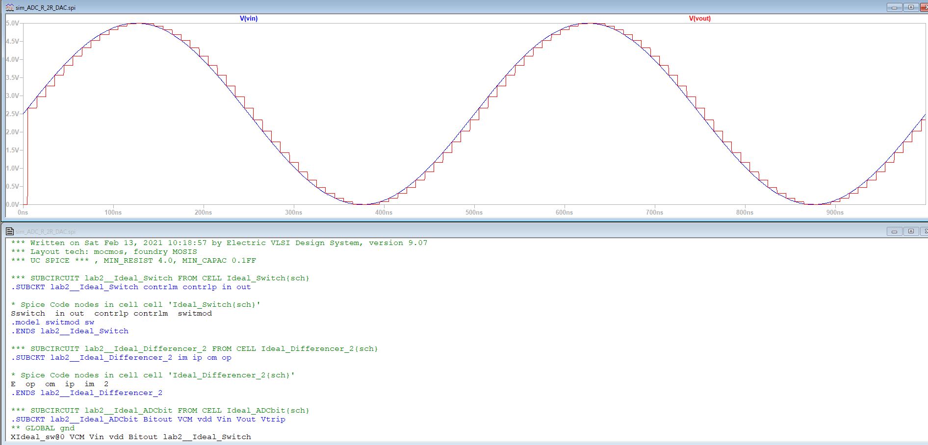
Figure 6. R-2R ladder LTSpice code and simulation.
Task 3
The time delay from the B9 pin when the DAC drives a 10pF load was
tested. B0-B8 pins were connected to ground and a 10pF load was added.
LTSpice simulated and verified the time delay to the calculated one.
TD = .7RC
TD = .7 (10k)(10p)
TD = 70ns
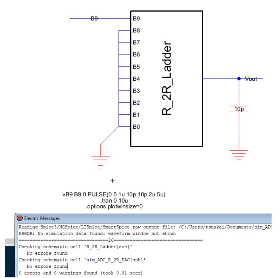
Figure 7. R-2R ladder with a 10pF capacitor.
The expected time delay was calculated to be
70ns. The simulation was probed at 1.25V and the output time delay was 72.3ns.
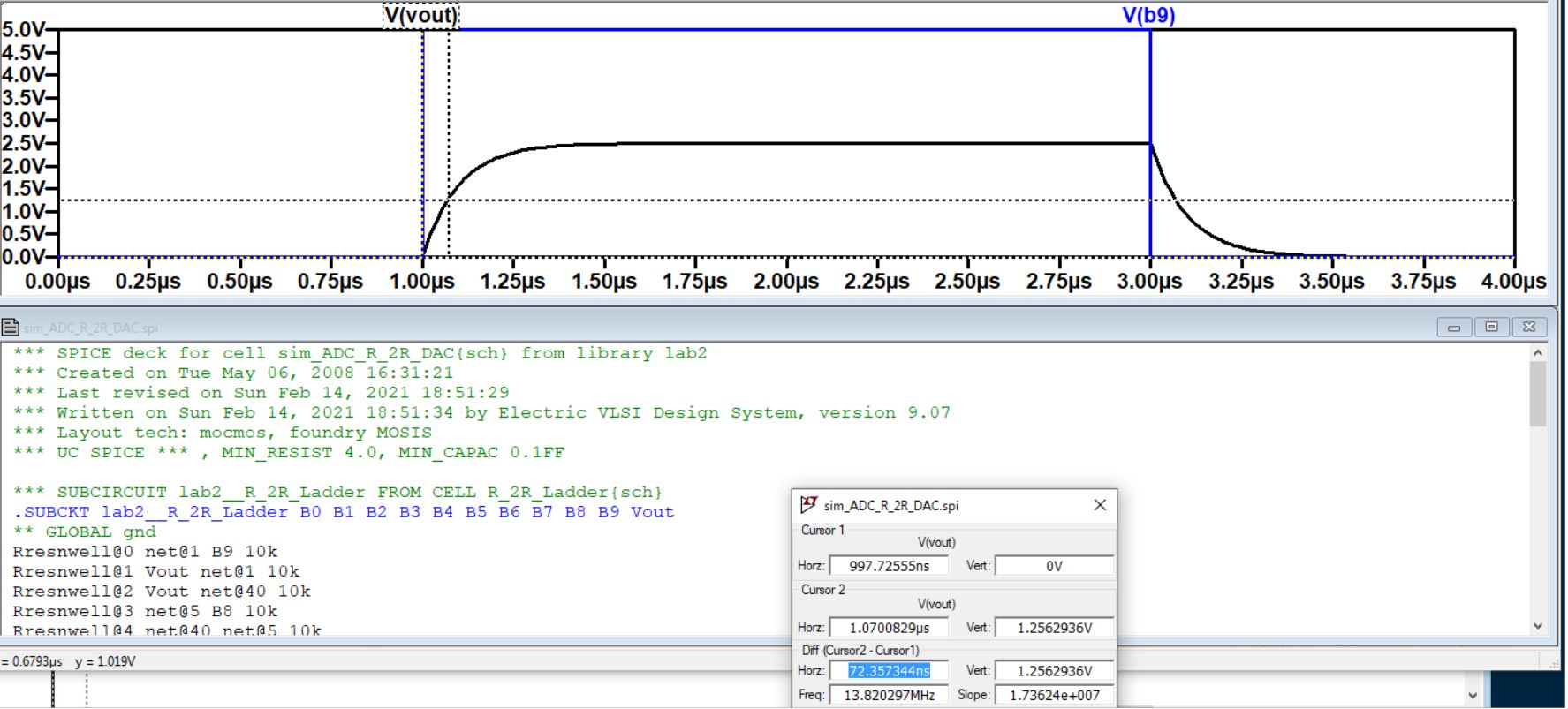
Figure 8. Verifying time delay with LTSpice.
2. Discussion
This lab introduced me to ElectriVLSI and allowed me to become familiar with the program. I gained more of an understanding of ADC and DACs.