ENGR338
2021 Spring
Final Project - 8-bit SAR ADC
Sophie Turner
sjturner@fortlewis.edu
8-bit SAR ADC
1. Introduction
This
purpose of this project was to create a 8-bit SAR block and simulate it
in LTSpice. Successive-Approximation Register (SAR) Analog to
Digital Converter (ADC) converts an analog waveform to a binary
output. The SAR ADC consists of five components: Sample/Hold block,
comparator, SAR logic block, 8-bit DAC, and a timing block. The
SAR finite state machine table in Figure 2 shows the algorithm that
each cycle steps through. The
8-bit SAR ADC was created using 3 input NAND gates and TI D flip
flops. LTSpice was used to create the components and simulate each
logic. 50 nanometer CMOS technology was used to create the design.
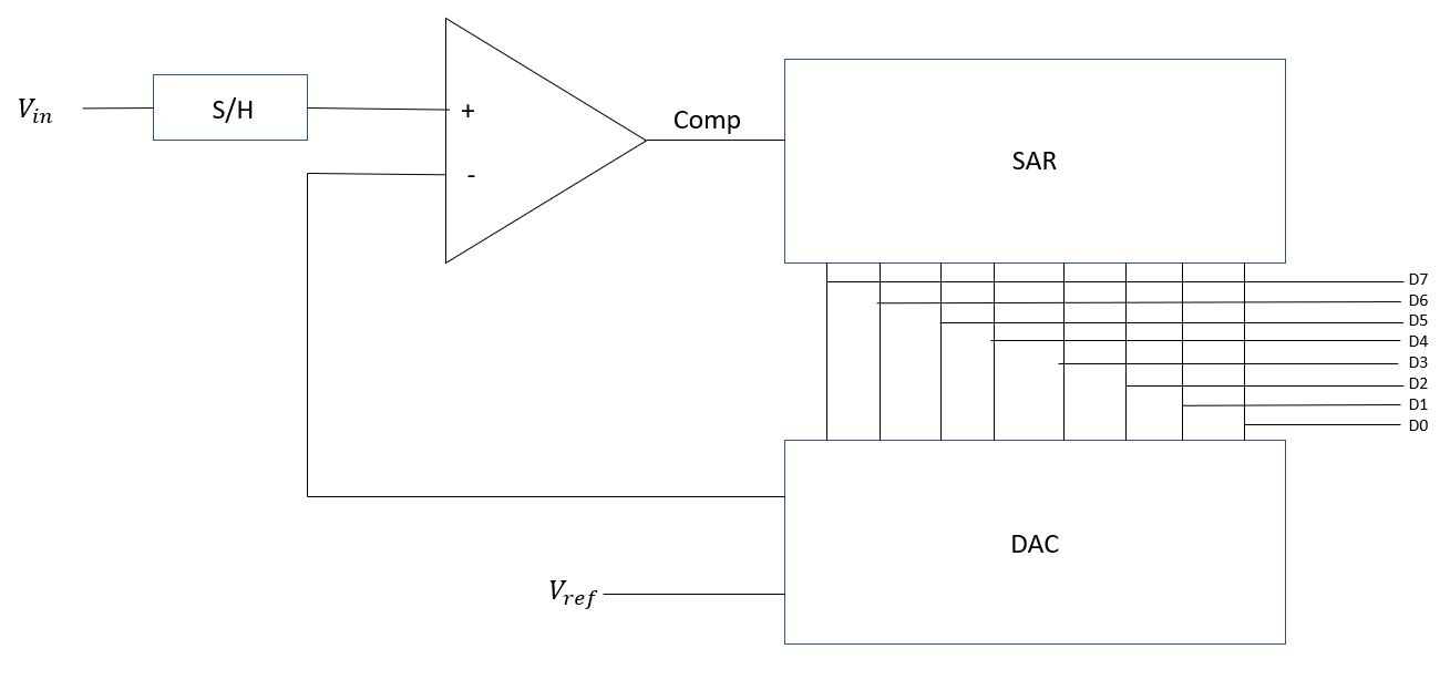
Figure 1. 8-bit SAR ADC
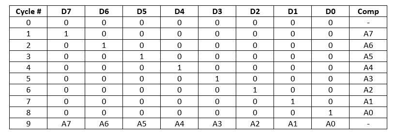
Figure 2. SAR Finite State Machine Algorithm
2. Methods
LTSpice was used to create the schematics and
simulate the design. A 3 input NAND gate, TI DFF, and an 8-bit SAR ADC were
created and simulated using 50n CMOS technology.
3. Results
3 input NAND gate
A 3 input NAND gate was created using 50n technology.
The 3 input NANDs were created for the TI DFF. For the 50n technology the PMOS
width=1u, length=50n, for NMOS width=0.5u and length=50n. A symbol was created
and simulated to verify the NAND logic as seen in Figure 4.
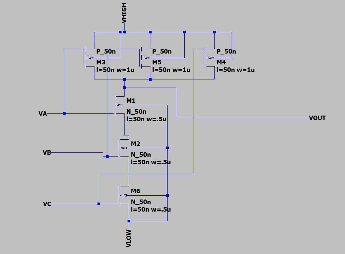
Figure 3. 3 input NAND schematic.
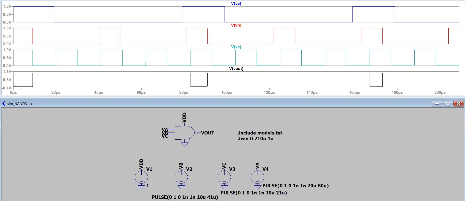
Figure 4. 3 input NAND simulation.
TI D flip flop
The
TI D flip flop was created using the 3 input NAND gates. An symbol for the
TI DFF was created and
simulated to verify the logic as seen in Figure 6 and Figure 7. When
the system is set with a '0' and reset='1' then '1' will be held in the
memory and outputted as seen in Figure 6. When reset='0' and set='1'
then the system will output '0' as seen in Figure 7.
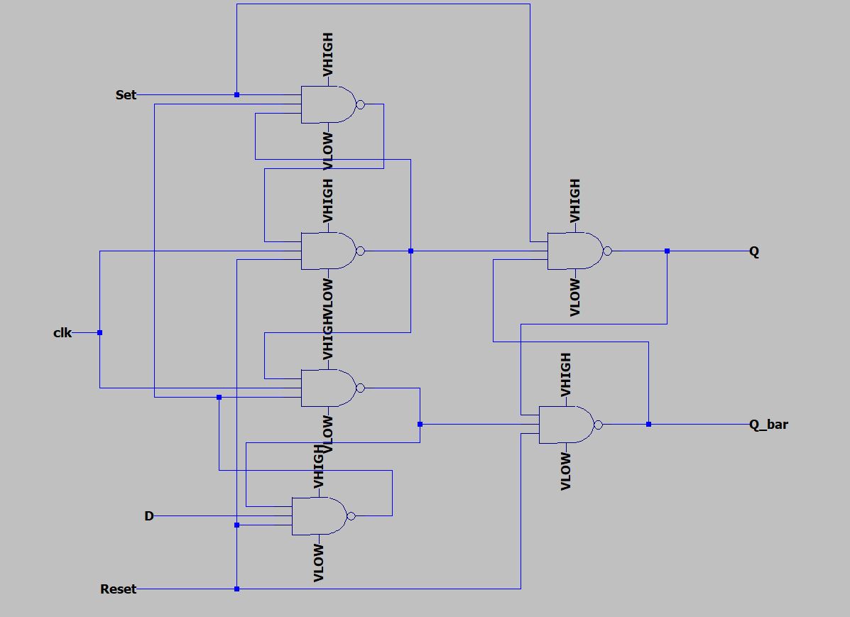
Figure 5. TI DFF schematic.
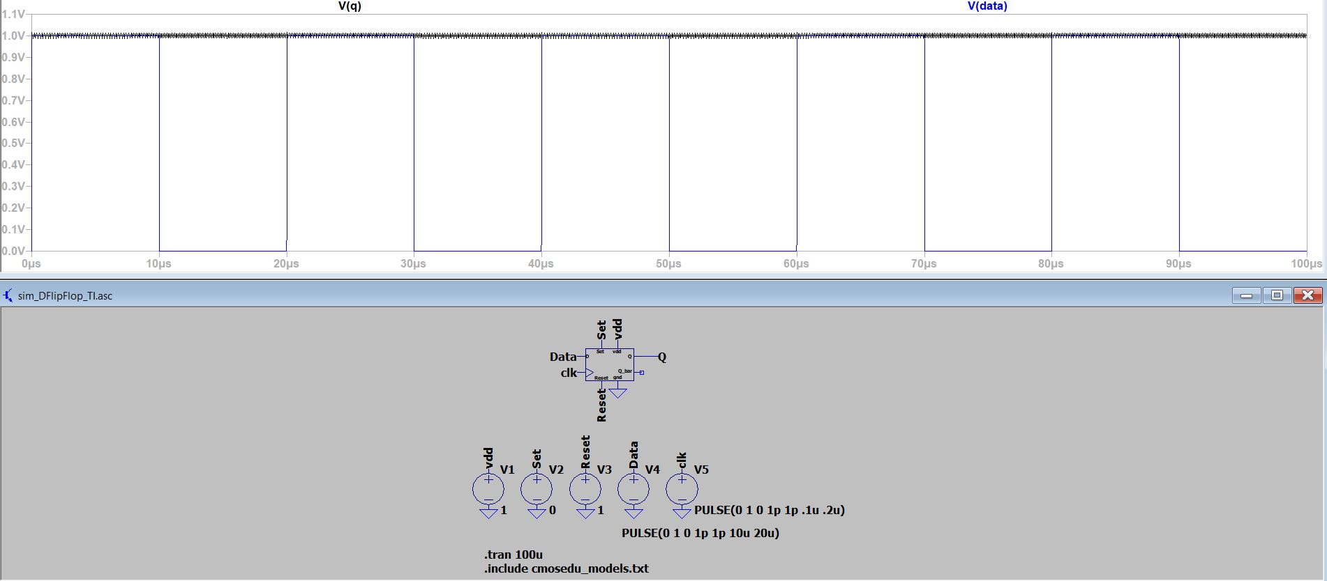
Figure 6. TI DFF simulation when Reset=1, Set=0.
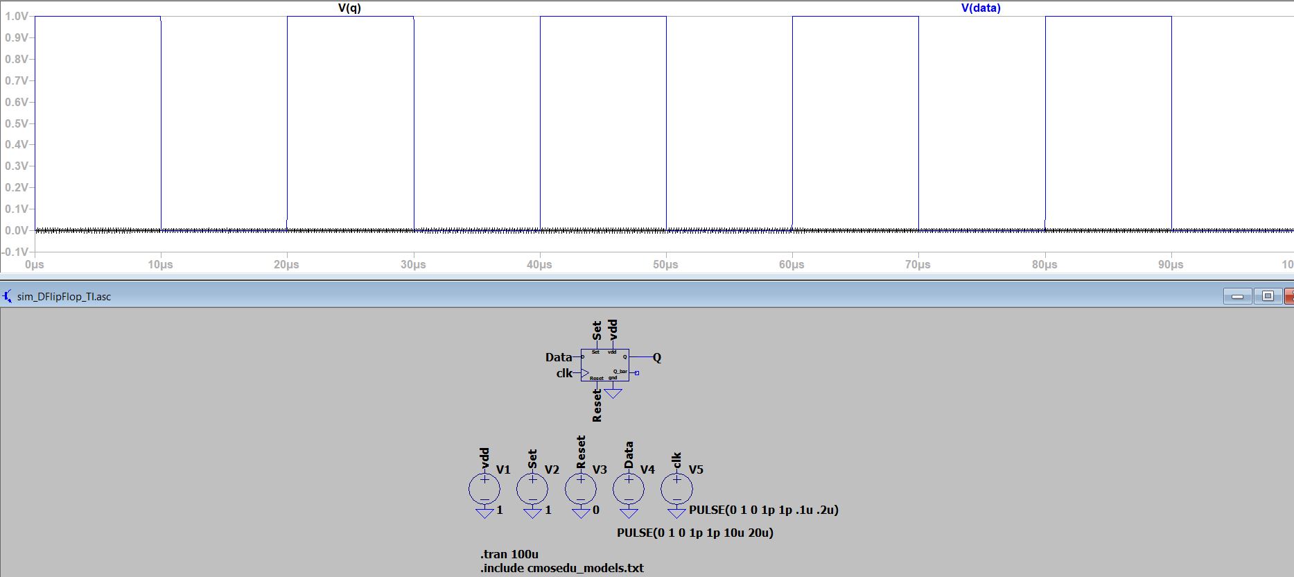
Figure 7. TI DFF simulation when Reset=0, Set=1.
8-bit SAR ADC
An 8-bit SAR ADC was created using TI DFF.
The TI DFF is used to create a shift register and sequencer. The shift
register shift to the different states and stores the states. The
sequencer compares the bits with the comparator and then outputs the
data serially. The 8-bit SAR ADC was simulated using LTSpice and the
logic was verified using different clock and comparator signals as seen
in Figures 9 and 10.
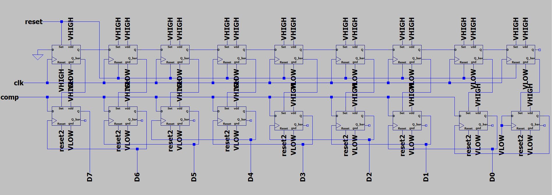
Figure 8. 8-bit SAR ADC schematic.
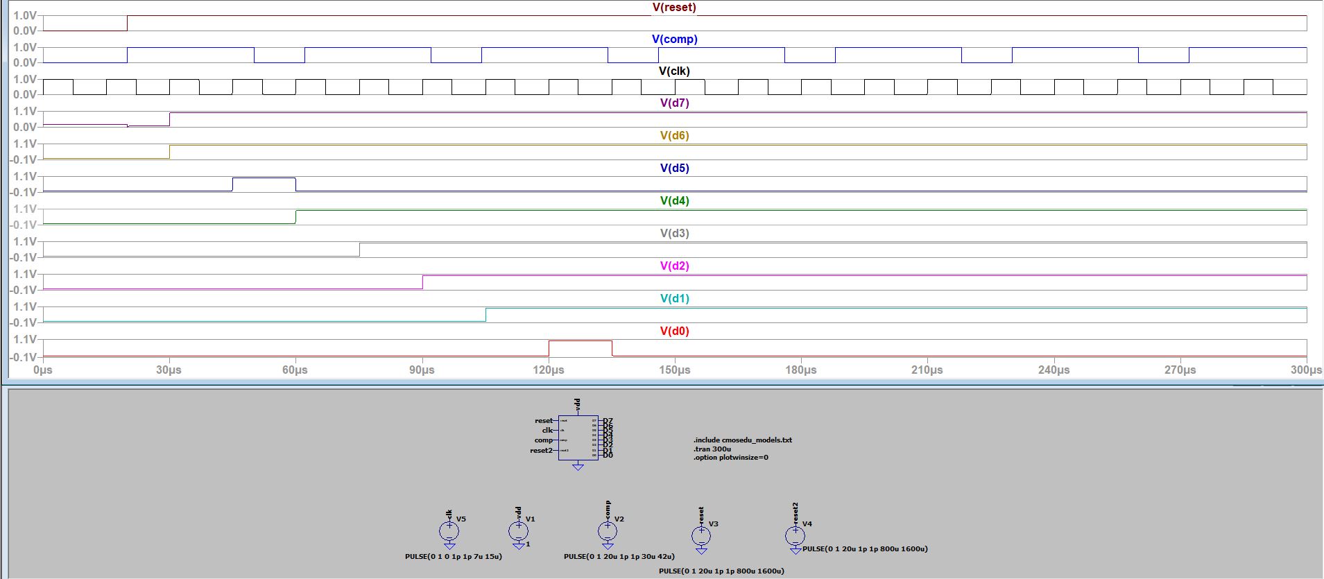
Figure 9. 8-bit SAR ADC simulation 1.
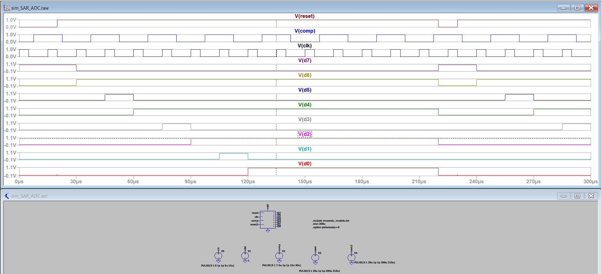
Figure 10. 8-bit SAR ADC simulation 2.
2. Discussion
This
project allowed us to learn more about SAR ADCs. We learned more about
the components within the SAR ADC, and we were able to verify the
functionality of the SAR ADC and TI DFF. We were able to use the
knowledge we gained from this semester and past courses to design and
verify this design.