ENGR338 Lab Spring 2021
Lab 7: Using Buses in ElectricVLSI
Scott Orban
SJOrban@fortlewis.edu
Introduction
The purpose of this lab was to learn how to use buses to create multi-bit logic devices using
Electric VLSI and
simulate them using
LTspice.
Materials and Methods
The circuits were built using Electric VLSI and simulated using
LTSpice .
Results
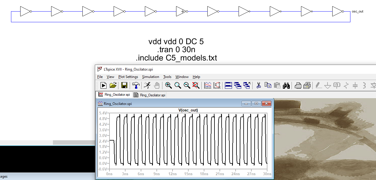
Figure 1: Basic Ring Oscilator schematic and simulation.
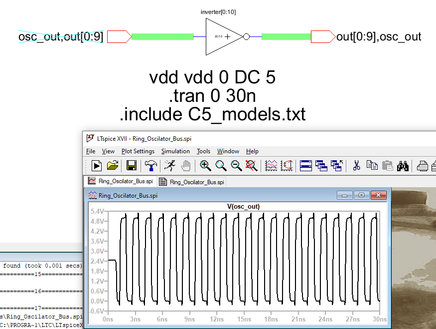
Figure 2: Ring oscilator with bus schematic and simulation.
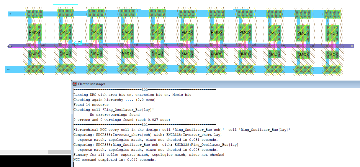
Figure 3: Ring oscilator layout.
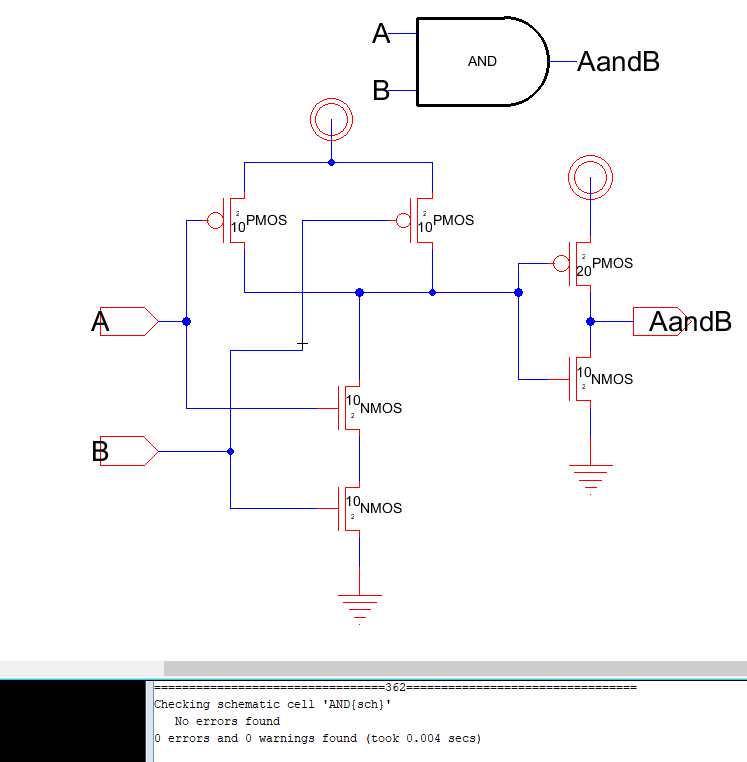 Figure 4: AND gate schematic.
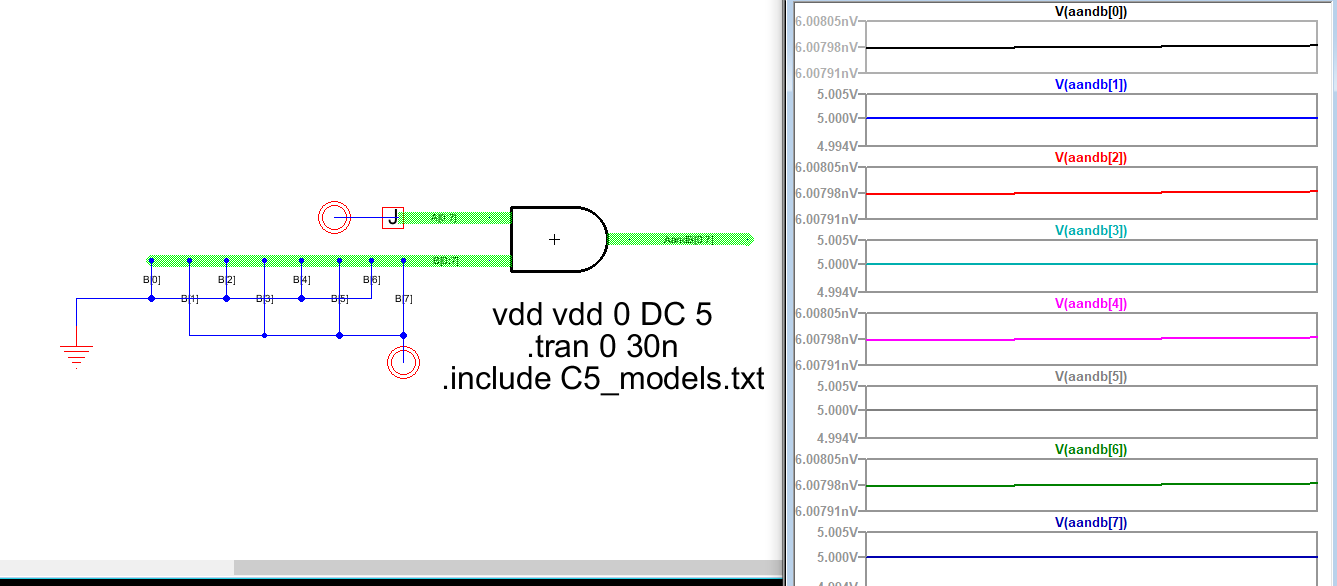 Figure 5: 8-bit AND gate simulation 1.
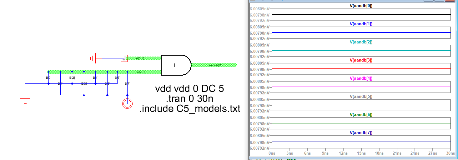 Figure 6: 8-bit AND gate simulation 2.
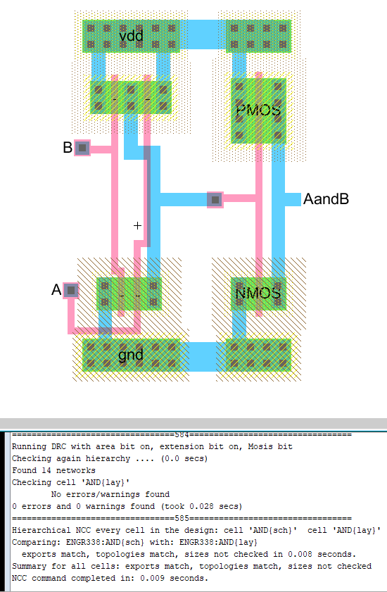 Figure 7: AND gate layout.
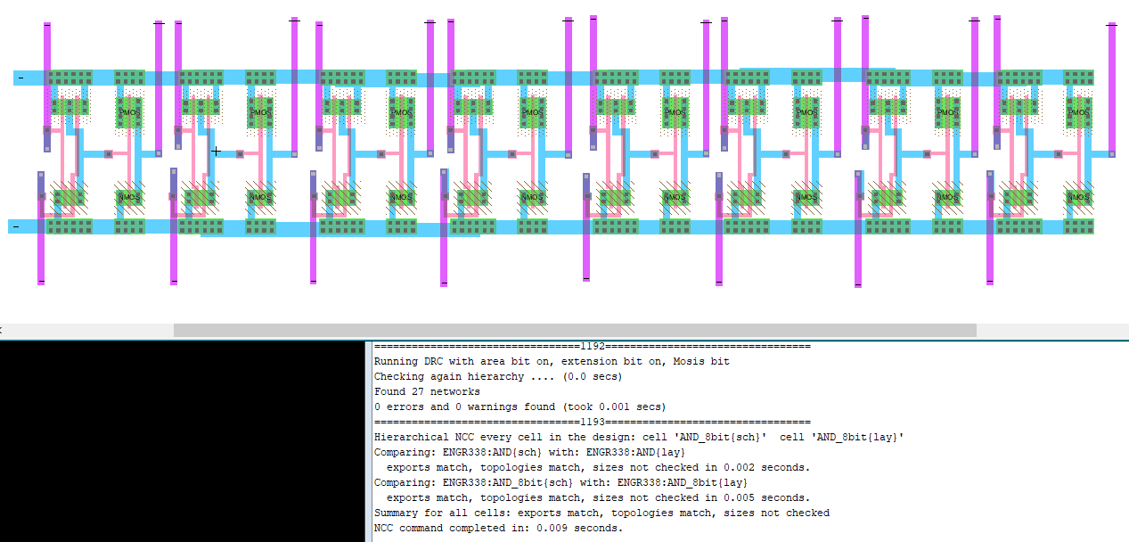 Figure 8: 8-bit AND gate layout.
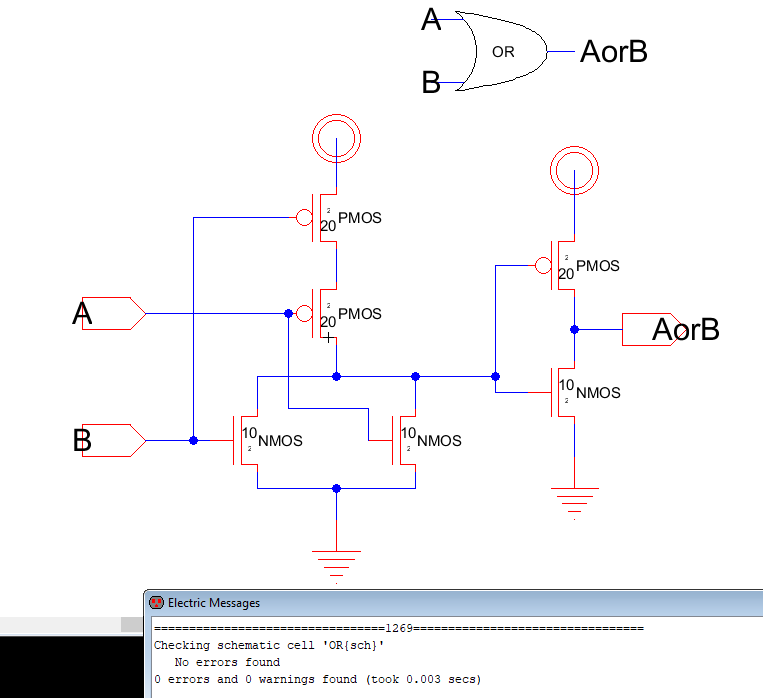 Figure 9: OR gate schematic.
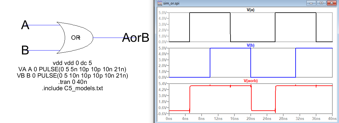 Figure 10: OR gate simulation.
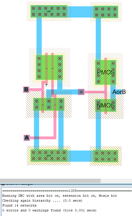 Figure 11: OR gate layout.
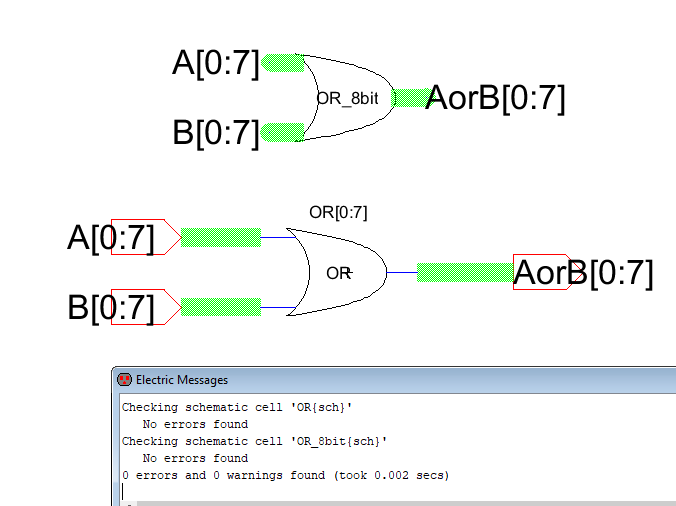 Figure 12: 8-bit OR gate with bus schematic.
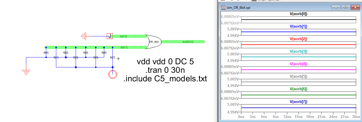 Figure 13: 8-bit OR gate with bus simulation.
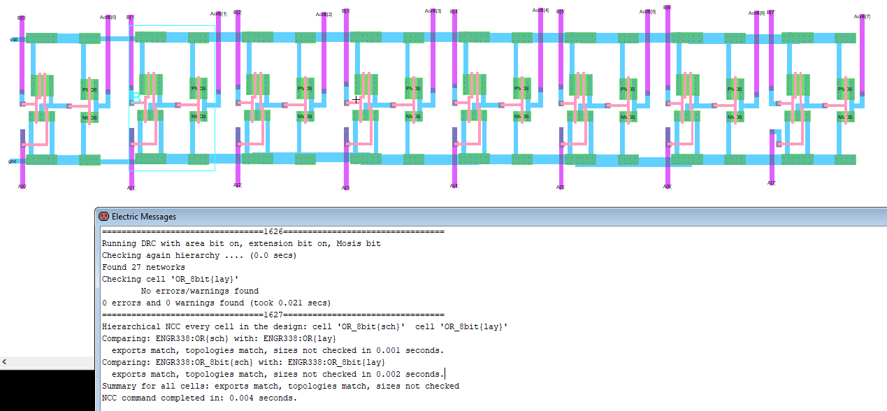 Figure 14: 8-bit OR gate layout.
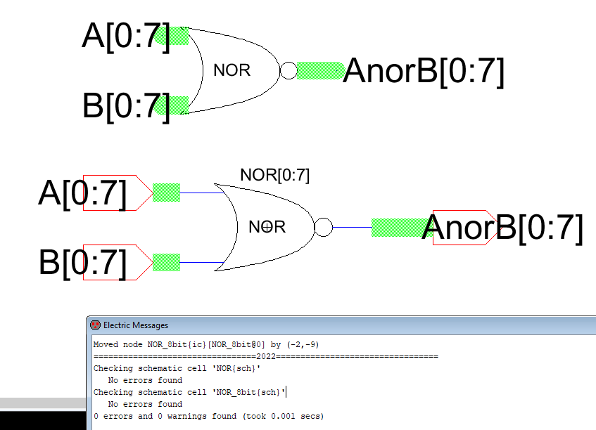
Figure 15: 8-bit NOR gate with bus schematic.
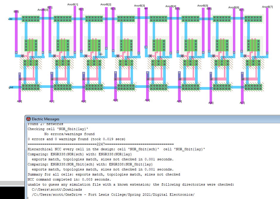
Figure 16: 8-bit NOR gate layout.
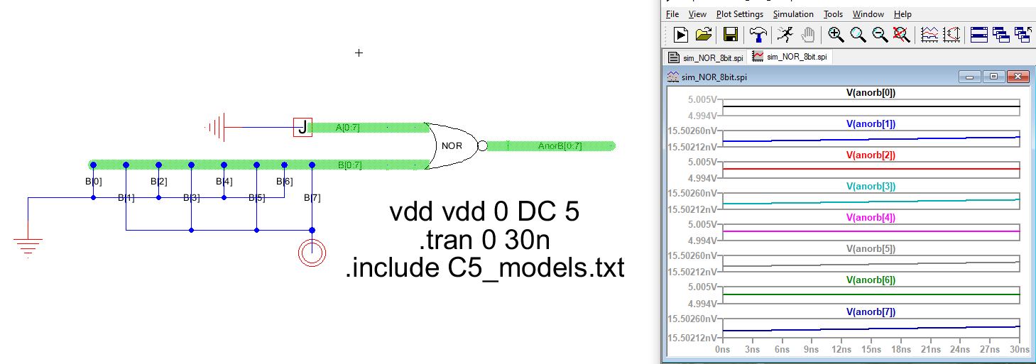
Figure 17: 8-bit NOR gate with bus simulation.
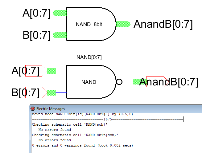
Figure 18: 8-bit NAND gate schematic with bus.
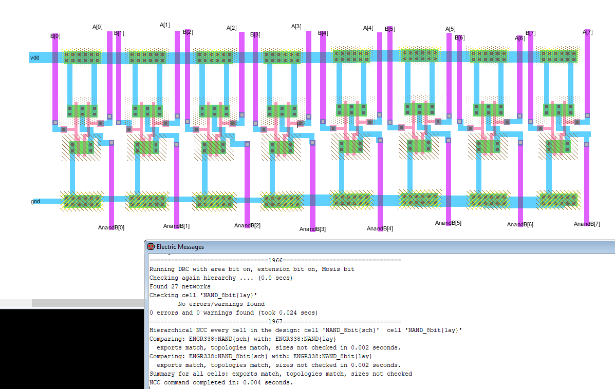
Figure 19: 8-bit NAND gate layout.
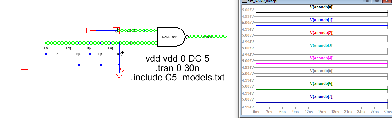
Figure 20: 8-bit NAND gate simulation.
The schematics and layouts matched and were error free, and the
simulation values were as expected.