ENGR338 Lab Spring 2021
Lab 6: The NAND, NOR, XOR, and Full Adder
Scott Orban
SJOrban@fortlewis.edu
Introduction
The purpose of this lab was to learn how to build a NAND, NOR, and XOR
gate then use those components to build a Full Adder using Electric
VLSI.
Materials and Methods
All components were built using Electric VLSI and simulated using
LTSpice.
Results
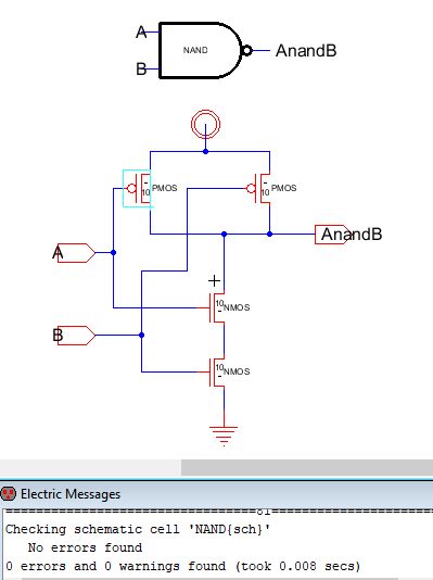
Figure 1: The schematic and icon
of the NAND gate.
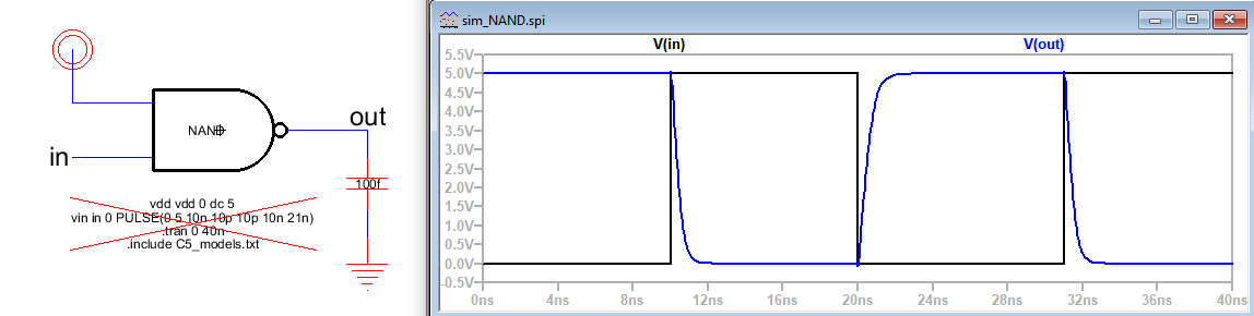
Figure 2: Verifying
the NAND gate logic using LTspice.
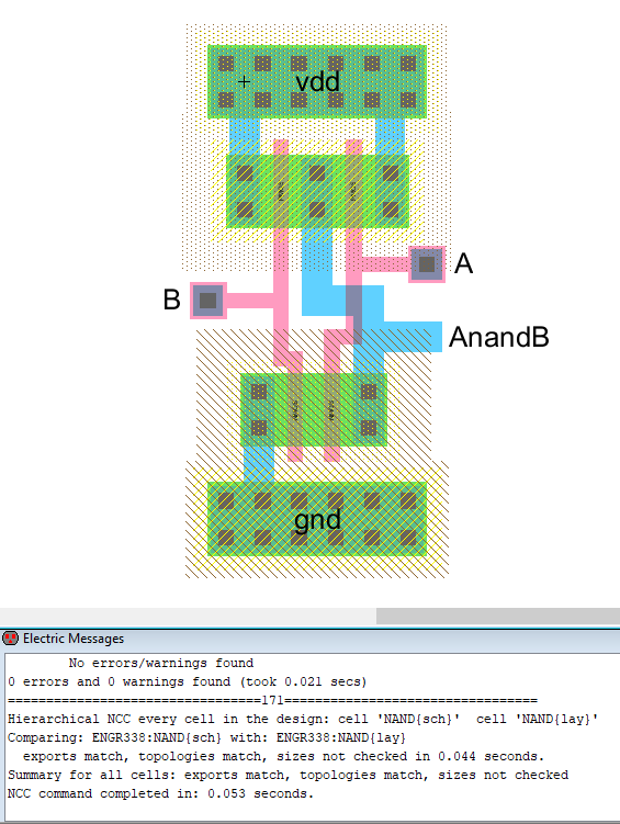
Figure 3: The layout of the NAND gate.
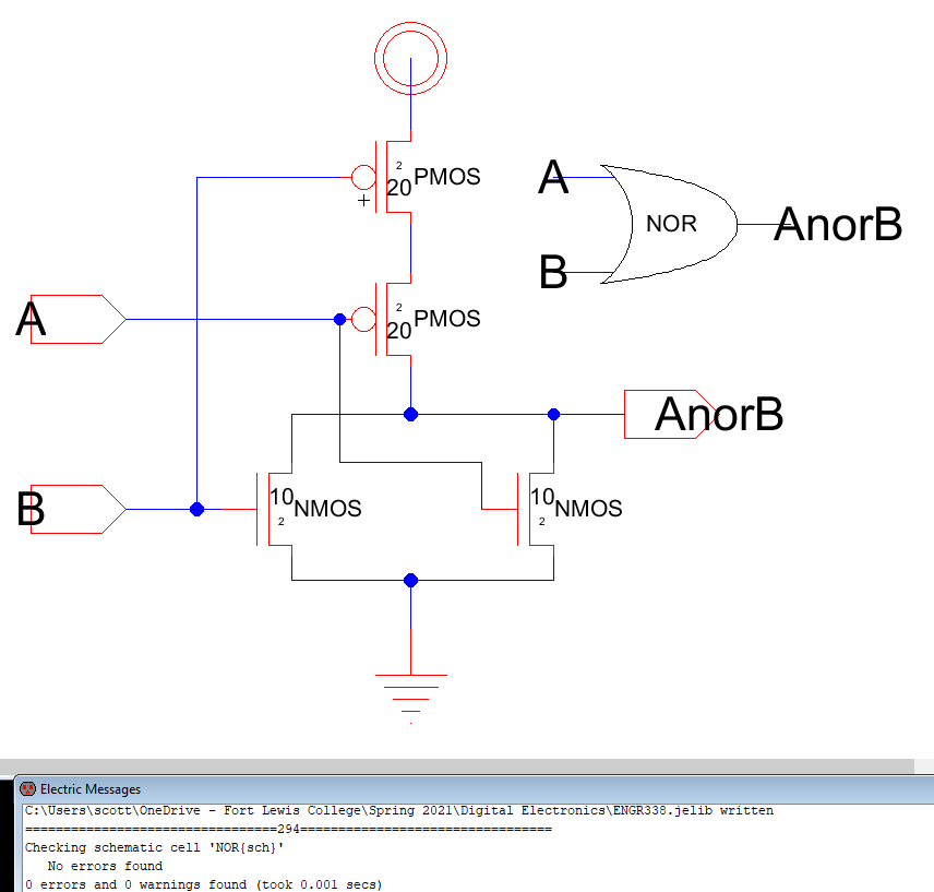 Figure 4: The schematic and
icon of the NOR gate.
Figure 4: The schematic and
icon of the NOR gate.
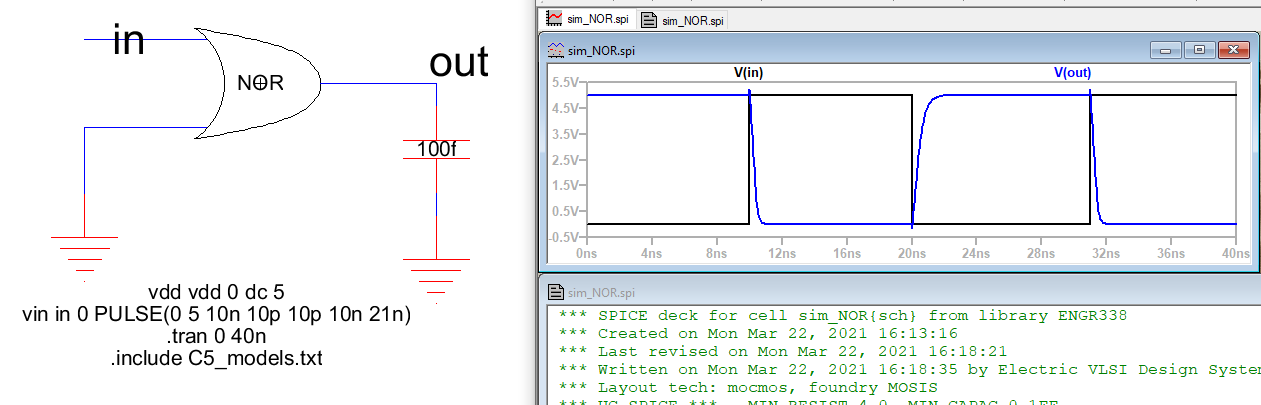 Figure 5: Verifying the NOR
gate logic using LTspice.
Figure 5: Verifying the NOR
gate logic using LTspice.
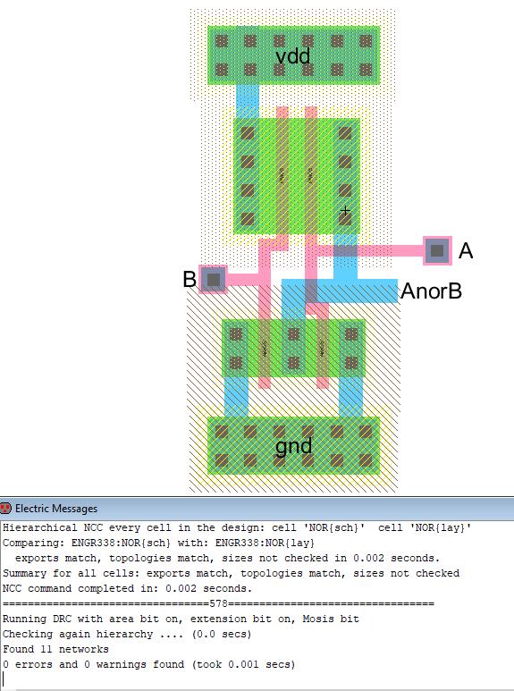 Figure 6: The layout of the NOR gate.
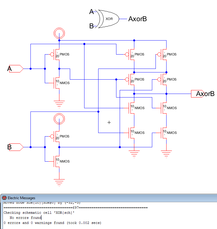 Figure 7: The schematic and
icon of the XOR gate.
Figure 7: The schematic and
icon of the XOR gate.
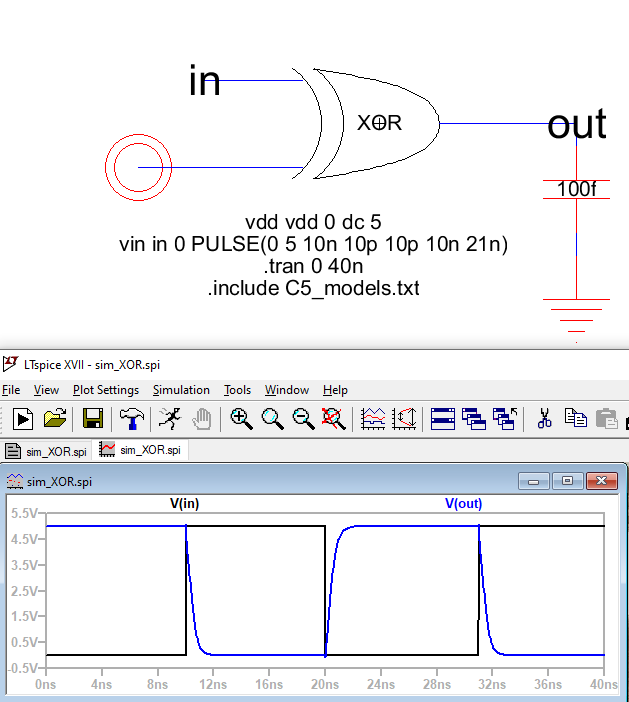 Figure 8: Verifying the logic of the XOR
gate using LTspice.
Figure 8: Verifying the logic of the XOR
gate using LTspice.
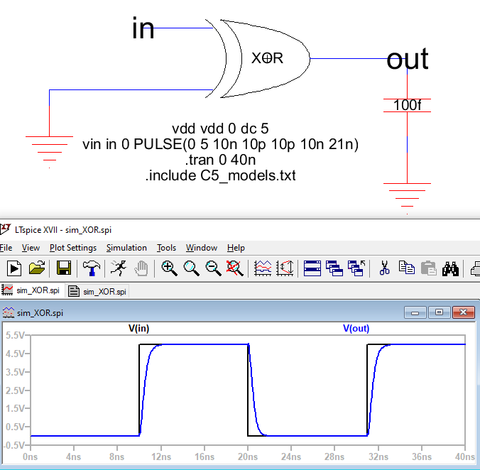 Figure 9: Verifying the logic
of the XOR gate using LTspice.
Figure 9: Verifying the logic
of the XOR gate using LTspice.
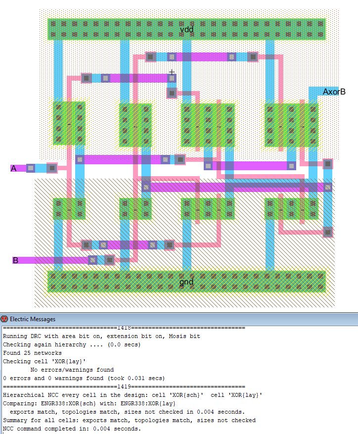 Figure 10: The layout of the
XOR gate.
Figure 10: The layout of the
XOR gate.
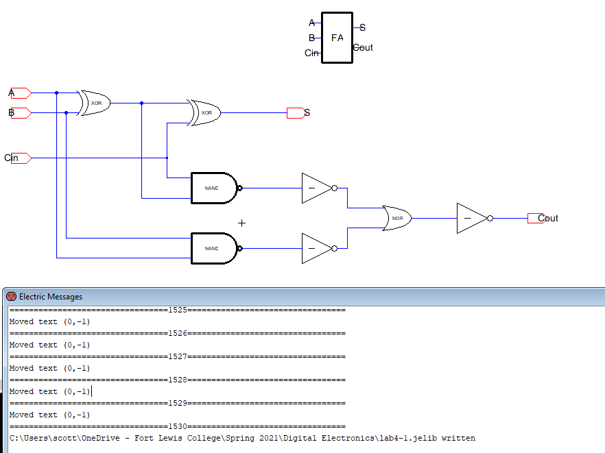 Figure 11: The schematic and icon of the Full
Adder.
Figure 11: The schematic and icon of the Full
Adder.
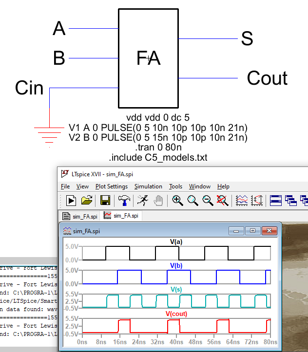 Figure 12: Verifying the
logic of the Full Adder.
Figure 12: Verifying the
logic of the Full Adder.
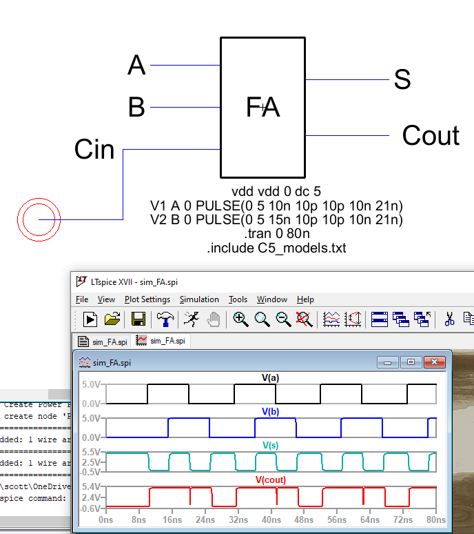 Figure 13: Verifying the
logic of the Full Adder.
Figure 13: Verifying the
logic of the Full Adder.
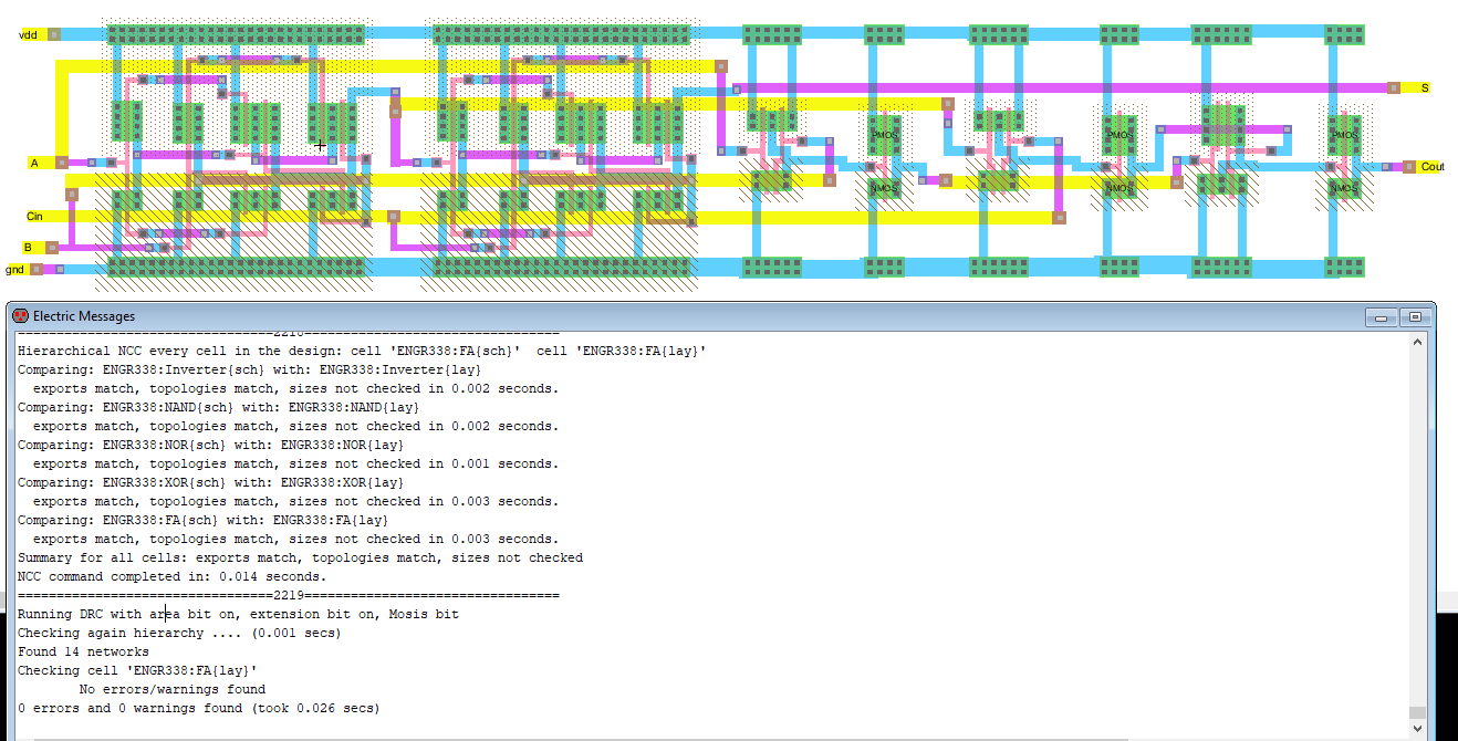 Figure 14: The layout of the
Full Adder using all the previously built layouts.
Figure 14: The layout of the
Full Adder using all the previously built layouts.
The schematics and layouts matched and were error free, and the
simulation values were as expected.