ENGR338 Lab Spring 2021
Lab 5: The inverter
Scott Orban
SJOrban@fortlewis.edu
Introduction
The purpose of this lab was to learn how to layout an inverter using Electric VLSI and simulate it using LTspice and IRSIM.
Materials and Methods
The inverters were built using Electric VLSI and simulated using
LTSpice and IRSIM.
Results
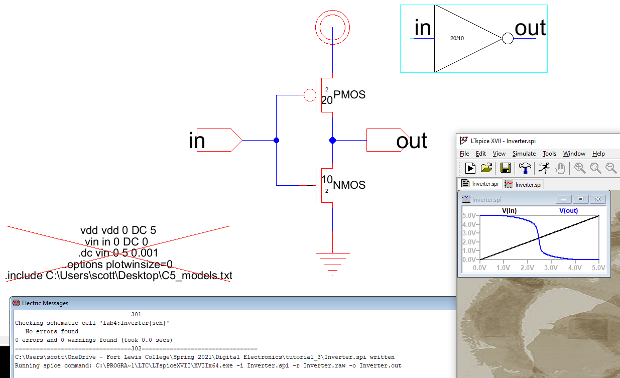
Figure 1: Inverter schematic with basic simulation.
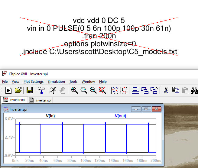
Figure 2: Simulation using the same schematic as figure 1, but with a pulse function as the input.
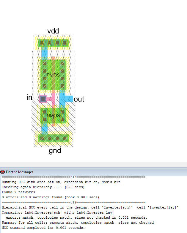
Figure 3: Layout of the inverter.
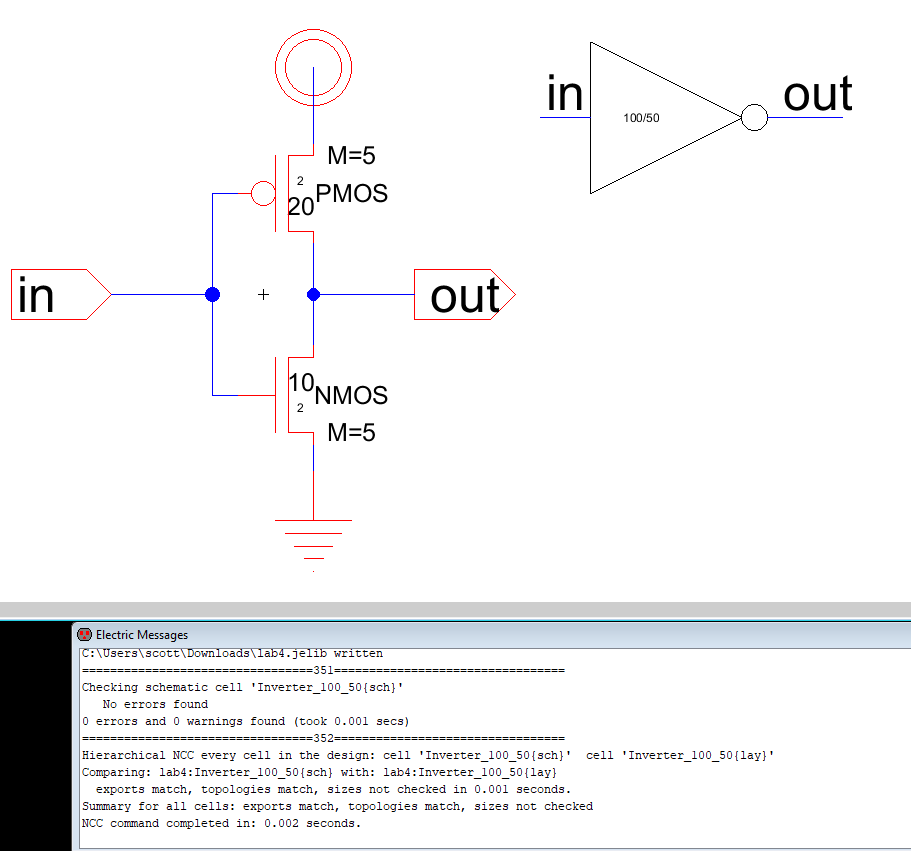 Figure 4: 100/50 inverter schematic.
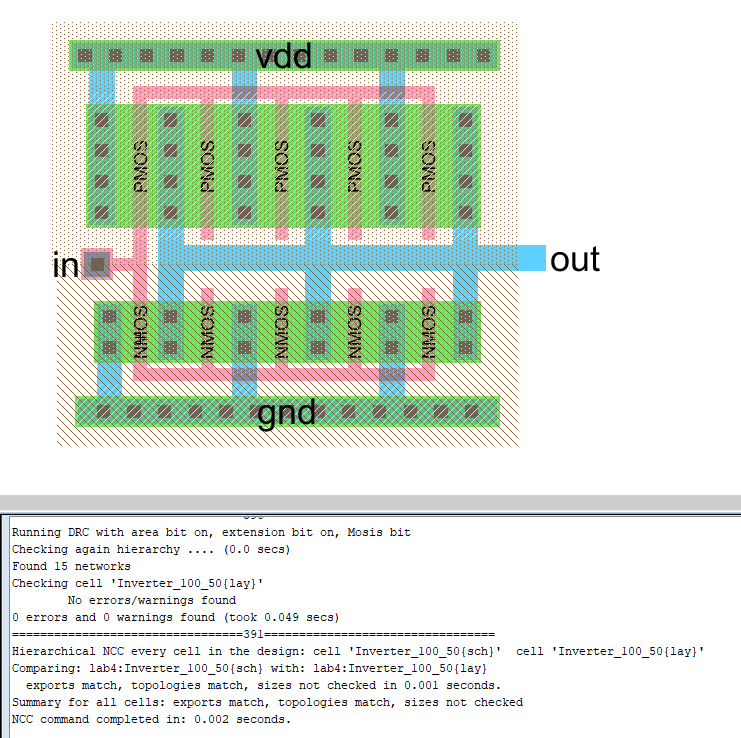 Figure 5: 100/50 inverter layout.
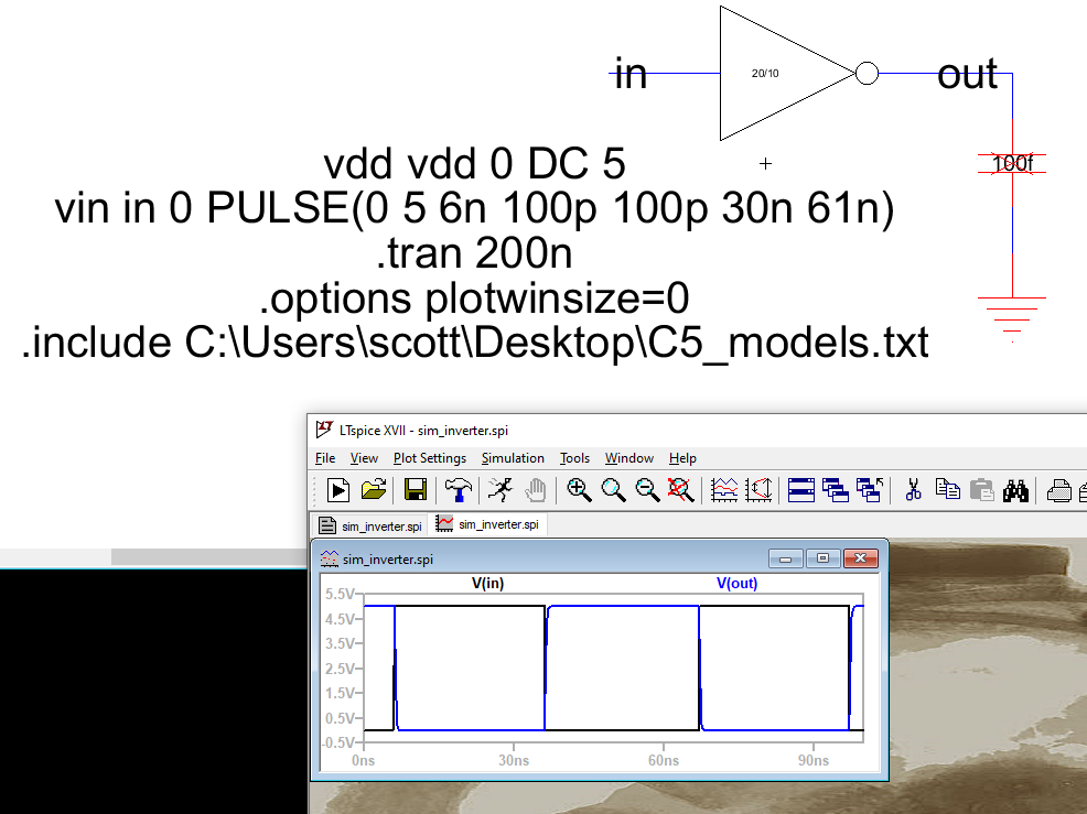 Figure 6: 20/10 inverter simulation with 100fF C load.
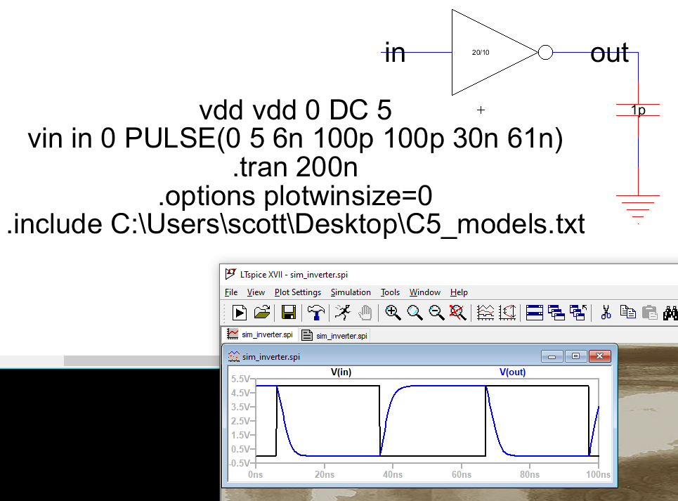 Figure 7: 20/10 inverter simulation with 1pF C load.
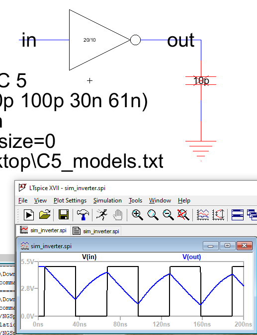 Figure 8: 20/10 inverter simulation with 10pF C load.
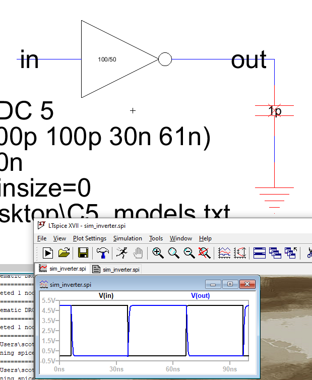 Figure 9: 100/50 inverter simulation with 1pF C load.
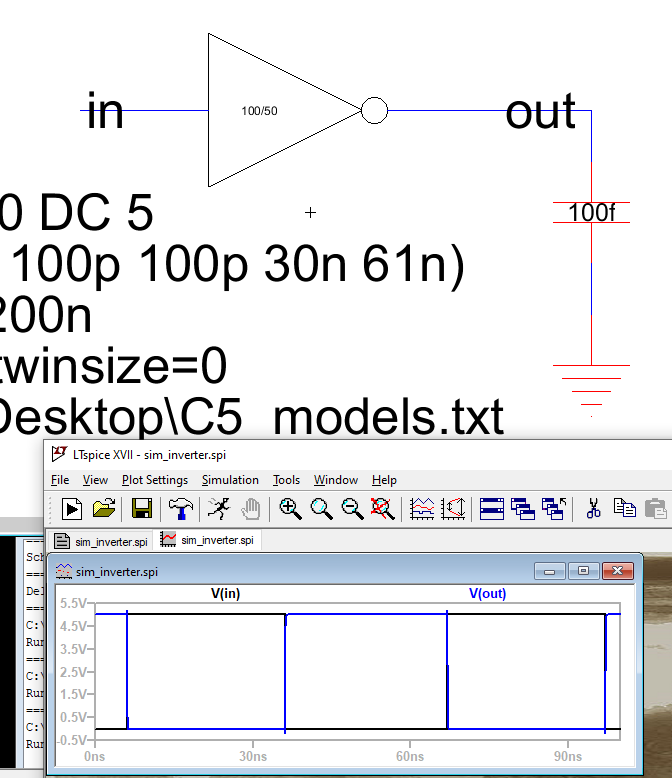 Figure 10: 100/50 inverter simulation with 100fF C load.
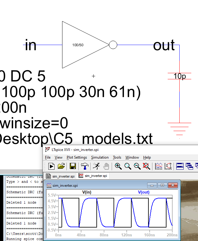 Figure 11: 100/50 inverter simulation with 10pF C load.
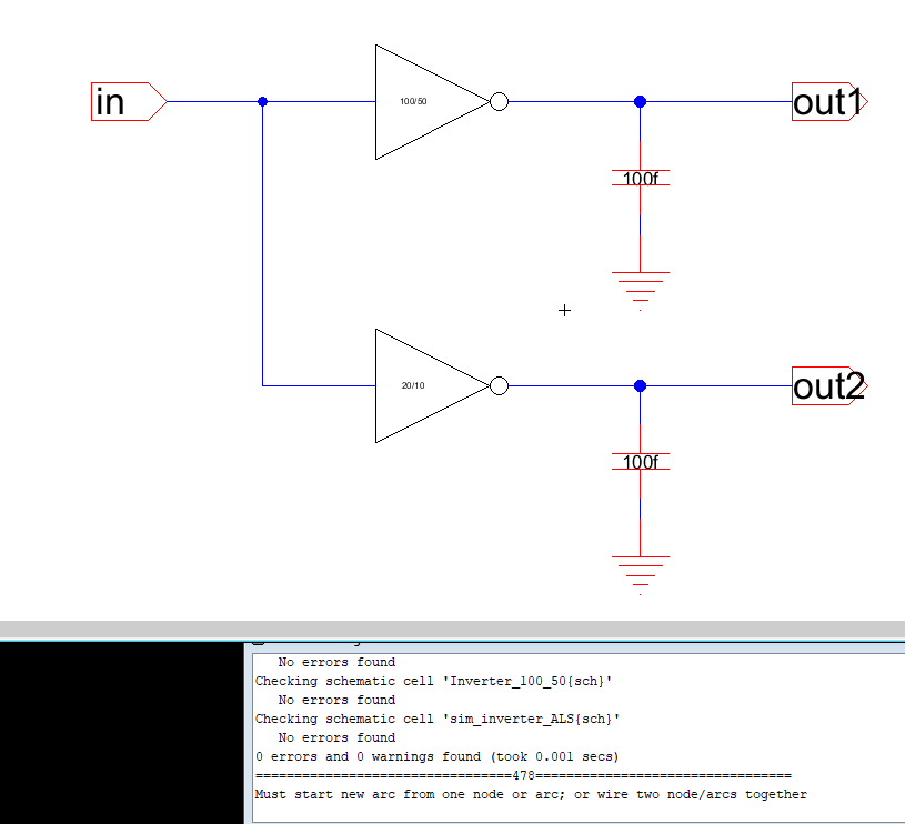 Figure 12: 100/50 and 20/10 inverter schematic for built in ALS and IRSIM simulation.
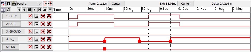 Figure 13: ALS simulation results.
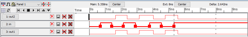 Figure 14: IRSIM simulation results.
The schematics and layouts matched and were error free, and the
simulation values were as expected.