ENGR338 Lab Spring 2021
Lab 2: Design an R-2R DAC
Scott Orban
SJOrban@fortlewis.edu
Introduction
The purpose of this lab was to look at the operation of an ideal ADC and DAC, and design an R-2R DAC to replace the ideal DAC.
Materials and Methods
The circuits were built using Electric VLSI and simulated using LTSpice.
Results
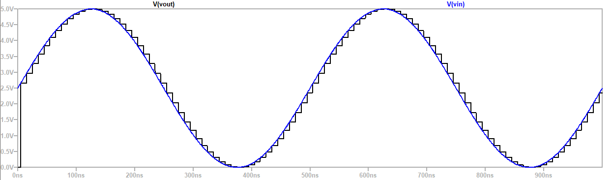
Figure 1: Simulated input and output of the ADC DAC circuit.
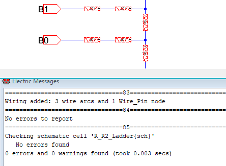
Figure 2: Error free R-2R ladder schematic.
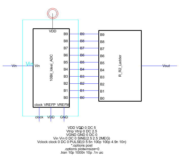
Figure 3: R-2R ladder ADC-DAC circuit.
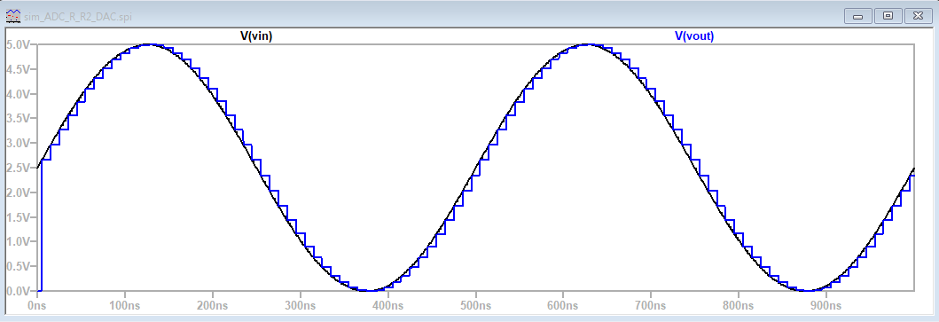
Figure 4: Simulated input and output of the R-2R ladder circuit.
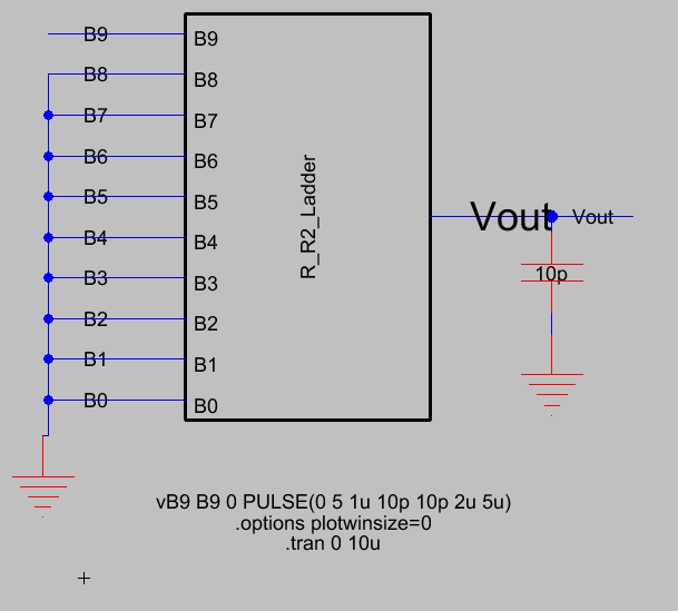
Figure 5: Time delay circuit of the R-2R circuit.
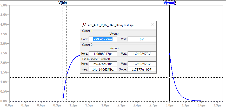
Figure 6: Time delay of the R-2R ladder DAC.
hand calculation: time delay = 0.7RC = 0.7 * 10k * 10p = 70ns
Discussion
The hand calculations and spice simulation values were the same.