Scott Orban
CE 351
HW1
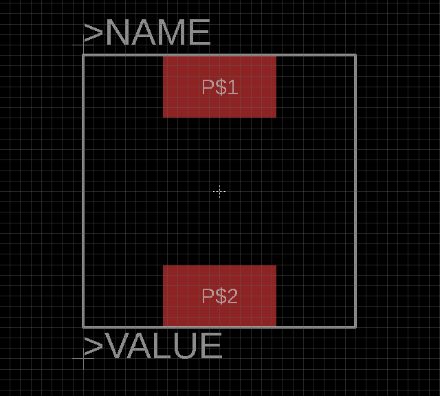
Figure 1: The footprint of the inductor.
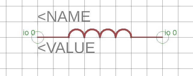
Fgure 2: The schematic view of the inductor.
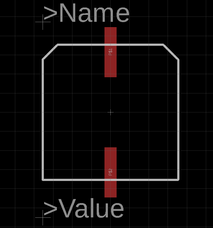
Figure 3: The footprint of the capacitor.
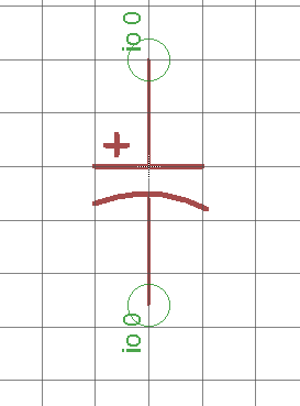
Figure 4: The schematic view of the capacitor.
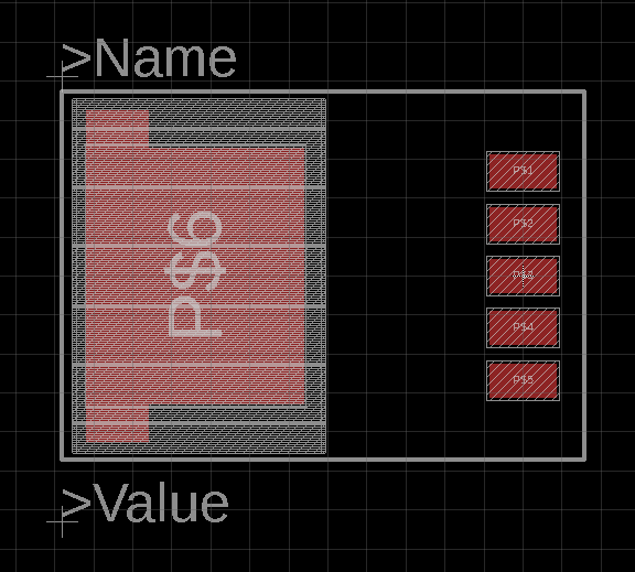
Figure 5: The footprint of the LM2596.
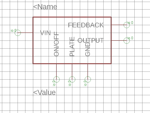
Figure 6: The schematic view of the LM2596.
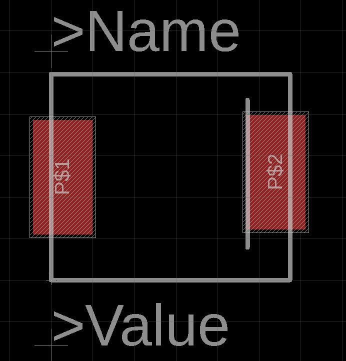
Figure 7: The footprint of the schottky diode.
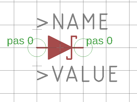
Figure 8: The schematic view of the schottky diode.
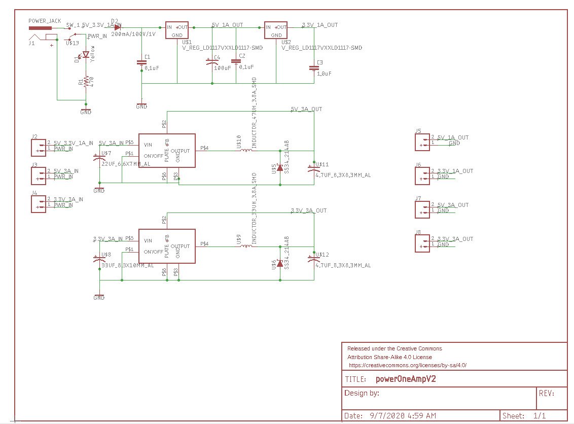
Figure 9: Schematic view of the PCB.
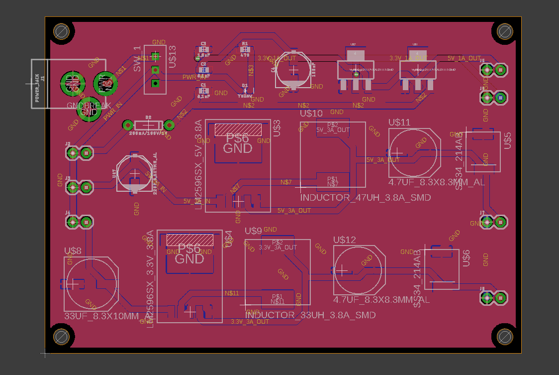
Figure 10: Layout view of the PCB.

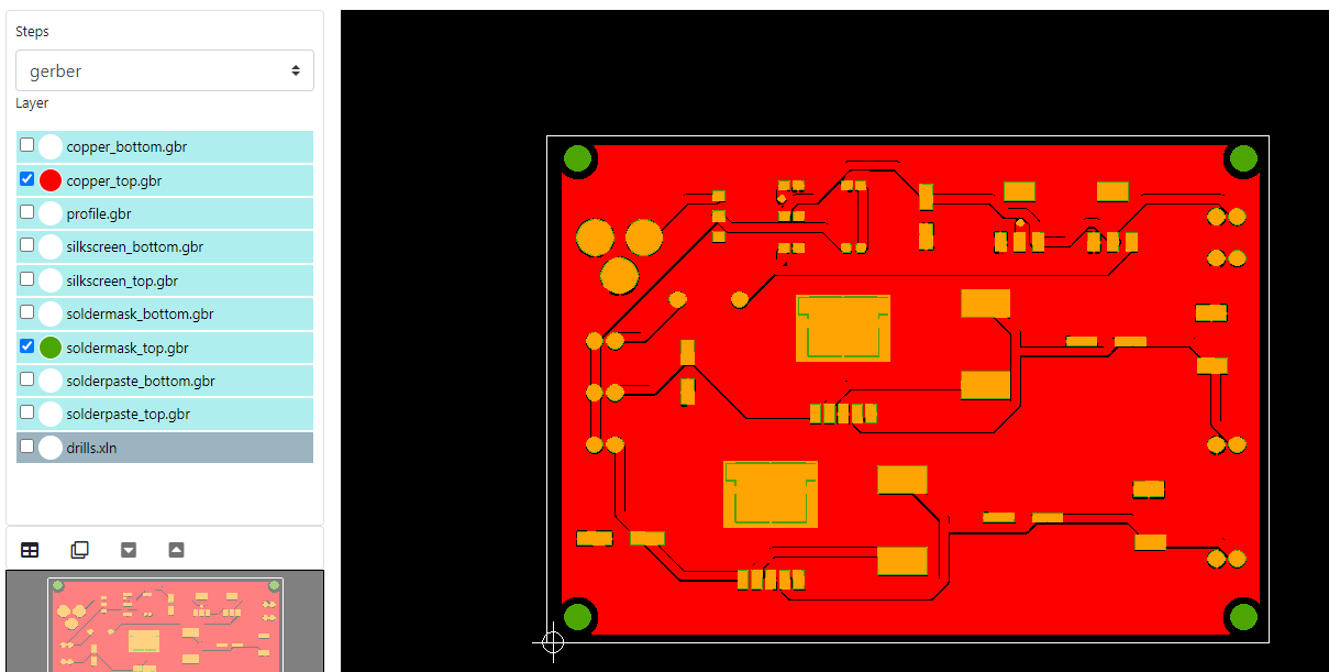
Figure 11: Gerber files uploaded to online gerber viewer.
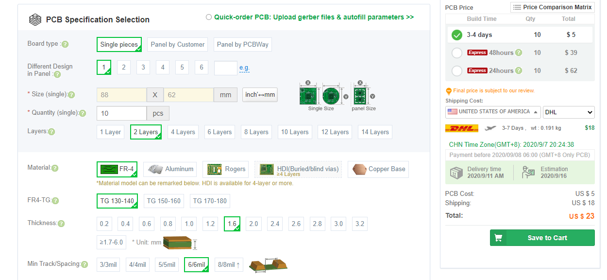
Figure 12: PCBway estimate.
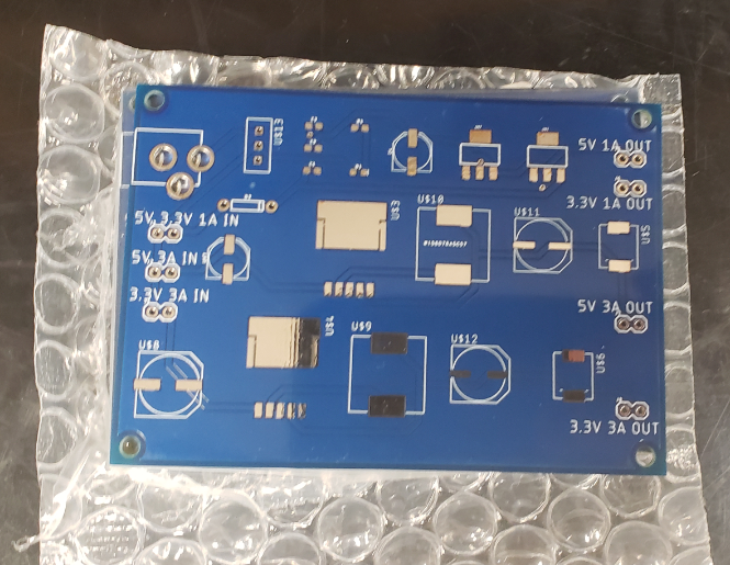
Figure 13: Bare PCB printed by PCBWay.
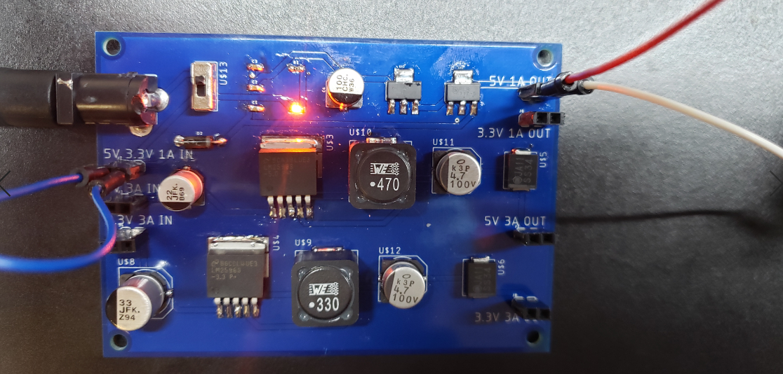
Figure 14: Power module set to 5V 1A.
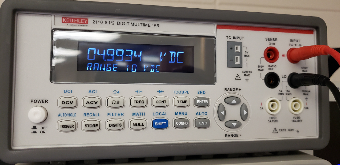
Figure 15: Output of the power module set to 5V 1A.
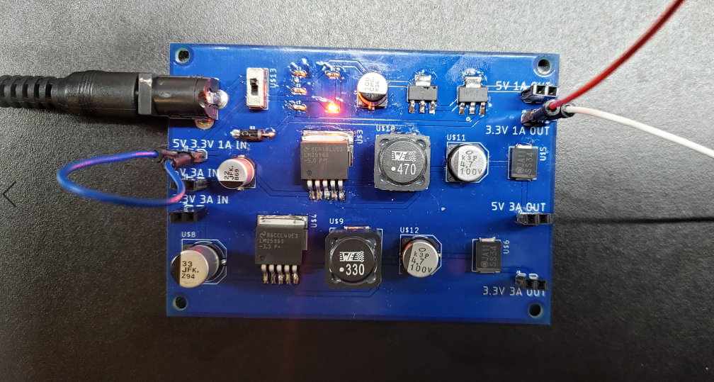
Figure 16: Power supply set to 3.3V 1A.
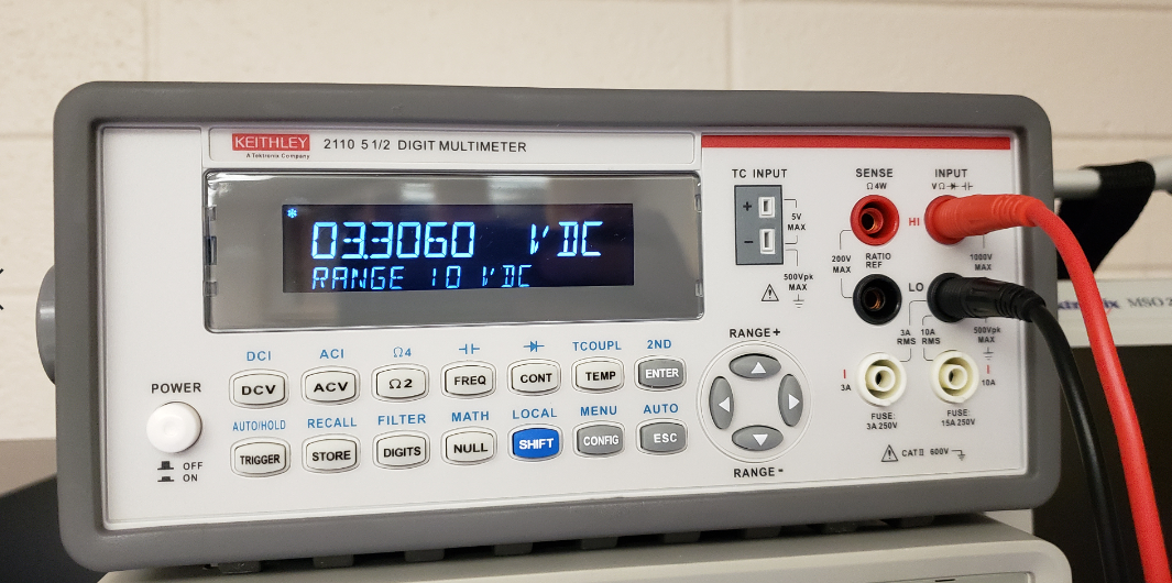
Figure 17: Output of the power supply set to 3.3V 1A.
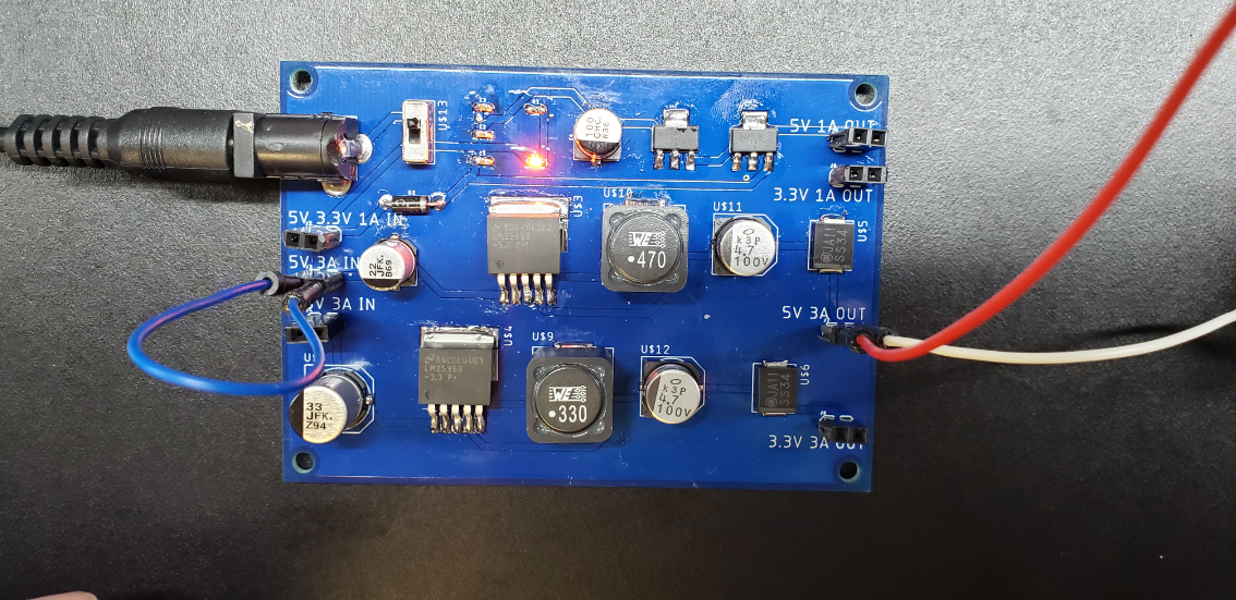
Figure 18: Power supply set to 5V 3A.
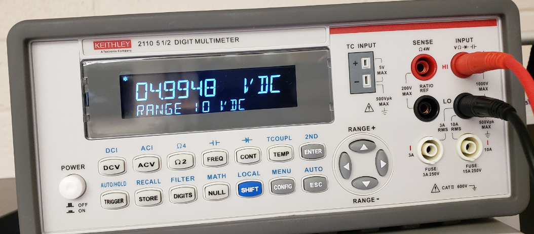
Figure 19: Output of power supply set to 5V 3A.
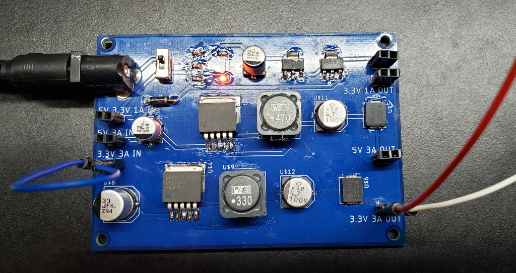
Figure 20: Power supply set to 3.3V 3A.
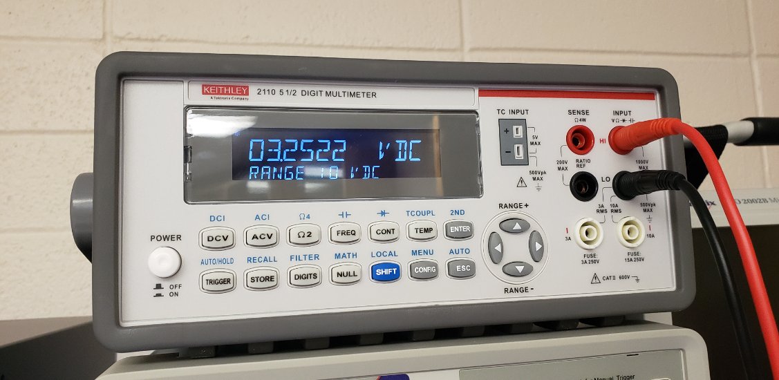
Figure 21: Output of power supply set to 3.3V 3A.