ENGR351 Lab 2020 Fall
Homework 1 -  DC Power Regulator PCB Design
Name:
Ryan Jeanes
Email: rejeanes@fortlewis.edu

Designing A DC Power Regulator
Introduction
From RTS modules, Wifi modules, SD reader modules, to the microcontrollers themselves, having a proper power supply is critical to ensure all of your modules are functioning properly. In this lab, we are designing a PCB using Eagle that will function as a DC power regulator, that will take a 7-18V input and output either 5V at 1A, 3.3V at 1A, 5V at 3A, or 3.3V at 3A.

Materials and Methods
The DC power regulator was designed in Eagle using the Sparkfun Eagle libraries. We made the designs for devices that were not available in Sparkfun's Eagle libraries. The list of materials is shown in Table 1, with the designed devices shown in Figures 1 through 5. The layout on the board was set
to prioritize  the ability to set traces from top to bottom to prevent conflicts with trace collision. 

Table 1 - List of parts used in the circuit design
Part (Part Number)
Quantity
3.3V/1A Regulator (NCP1117ST33T3G)
1
5V/1A Regulator (NCP1117ST50T3G)
1
0.1uF Capacitor (C0603C104Z3VACTU)
2
1.0uF Capacitor (CL10A105KP8NNNC)
1
100uF Capacitor (EEE-HC1C101XP)
1
LED (LTST-C191KFKT)
1
470 Ohm Resistor (RC0603JR-07470RL)
1
1KV/1A Diode (1N4007-TP)
1
1P2T SPDT Vertical Slide Switch
1
DC Barrel Power Jack (PJ-202A)
1
22uF Capacitor (EEE-FK1J220XP)
1
33uF Capacitor (EEE-FK1J330P)
1
4.7uF Capacitor (UUX2A4R7MCL1GS)
1
40V/3A SMC Shottky Diode (SS34)
1
47uH 3.8A 60mOhm Inductor (7447709470)
1
3.3V/3A Regulator (LM2596)
1
5V/3A Regulator (LM2596)
1
33uH 4.2A 45mOhm Inductor (7447709330)
1

Fig 1 - Footprint for the 33uH and 47uH inductors.
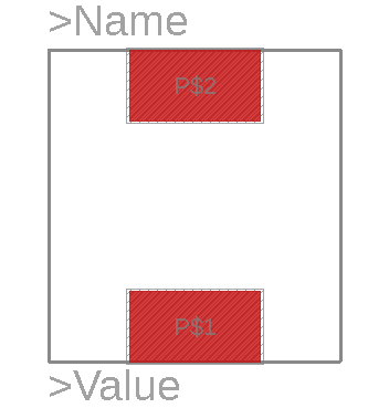
Fig 1 - Footprint created for 33uH and 47uH inductors


Fig 2 - Schottky Diode SMD footprint
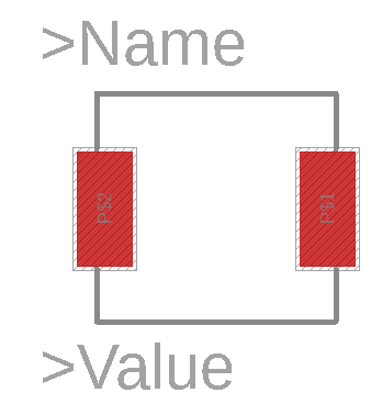
Fig 2 - Footprint created for Schottky Diode SMD


Fig 3 - Footprint for 4.7uF and 33uF capacitors
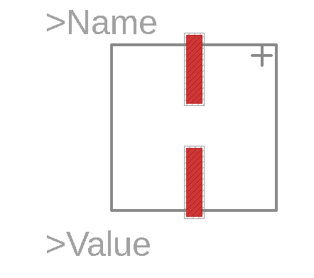
Fig 3 - Footprint created for 4.7uF and 33uF capacitors.


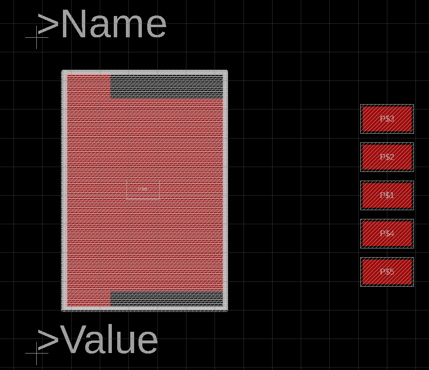
Fig 4 - Footprint created for both LM2596 voltage regulators


Fig 5 - Footprint created for SPDT switch

Results (Your data/figure should have a caption. Figures should be labeled/numbered.)
The final schematic, board design, and silkscreen layers are shown in Figures 6, 7, and 8, respectively. The design was fabricated and soldered as shown in Figure 9. The final design after soldering did not function as intended. The 5V/1A output pins pushed approximately 3.3V at 3.2mA and the 3.3V/1A output pins pushed approximately 2.4V at 2.3mA. The 5V/3A did not output any current or have any voltage potential across the pins and the 3.3V/3A output pins pushed 76.3mV at 27.3ľA. The components on the board were checked for secure solder connections and some components resoldered, but the outputs remained the same.

Fig 6 - Final Schematic for DC regulator
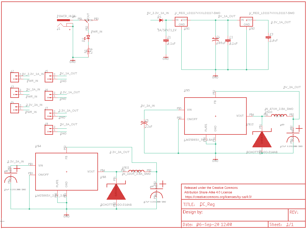
Fig 6 - Final schematic for DC regulator.

Fig 7 - Final board design for DC regulator
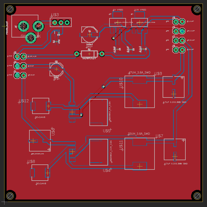
Fig 7 - Final board design for DC regulator.


Fig 8 - Silkscreen layer for the DC regulator
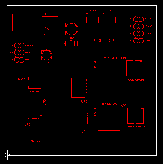
Fig 8 - Silkscreen for DC regulator

Fig 9 - Final Board
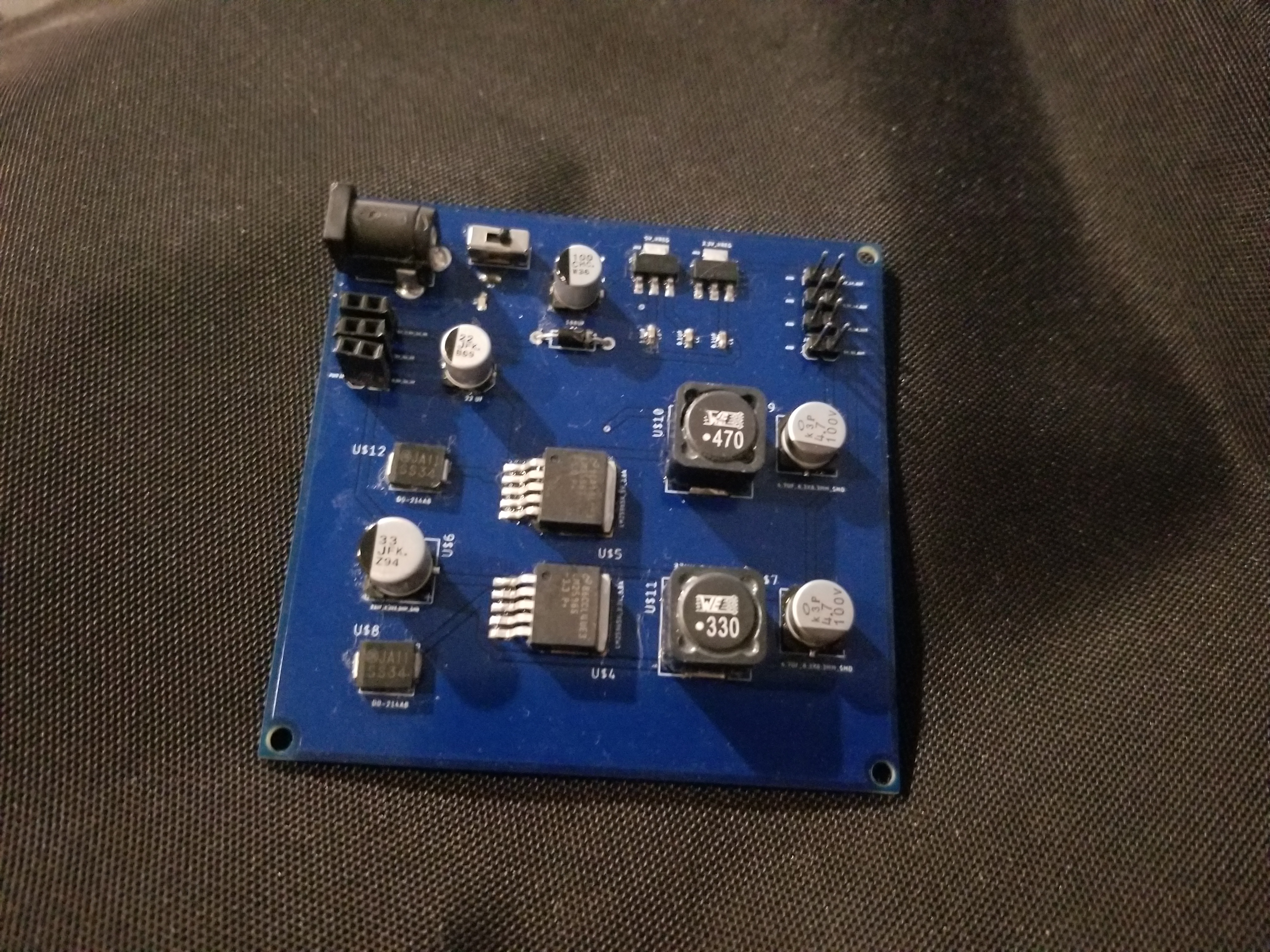
Fig 9 - The final soldered board.

Discussion
The design did not function as intended, either due to poor connections, improper design, or damaged components. Other than building a board that actually works, things that can be improved on the design is having the PWR in pins being male headers to allow for a jumper to be attached, with the output pins
being female header pins.