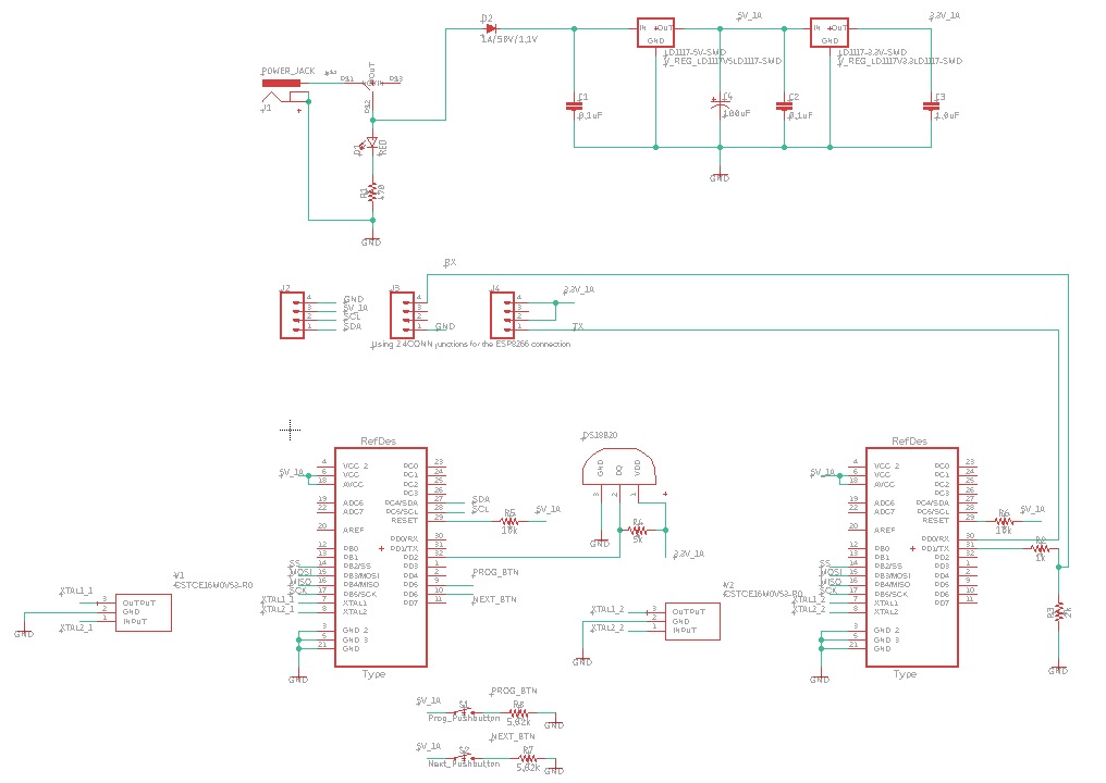
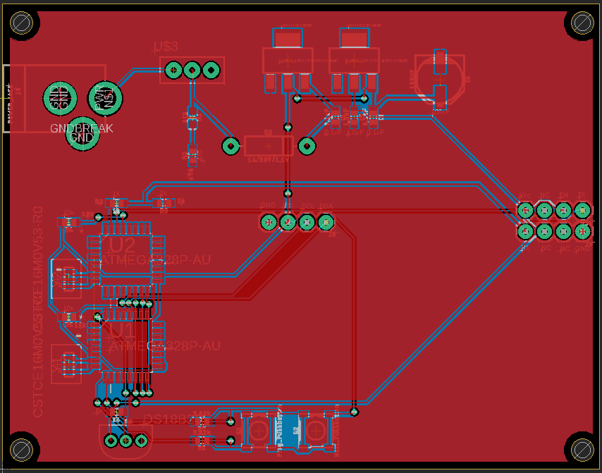
Figure 1 - Schematic of the board used in this project
| Part |
Quantity |
| DC Barrel Power Jack (PJ-202A) |
|
| 3.3V/1A Voltage Regulator (NCP1117ST33T3G) |
1 |
| 5V/1A Voltage Regulator (NCP1117ST50T3G) |
1 |
| 0.1uF Capacitor (C0603C104Z3VACTU) |
2 |
| 1.0uF Capacitor (CL10A105KP8NNNC) |
|
| 100uF Capacitor (EEE-HC1C101XP) |
1 |
| LED (LTST-C191KFKT) |
1 |
| 470 Ohm Resistor (RC0603JR-07470RL) |
1 |
| 1kOhm Resistor (2997-CR16102JTR-ND) |
1 |
| 2kOhm 0603 resistor |
1 |
| 5kOhm 0603 resistor |
1 |
| 10kOhm resistor (13-RE0603BRE0710KLTR-ND) |
1 |
| 1KV/1A Diode (1N5007-TP) |
4 |
| 1P2T SPDT Vertical Slide Switch |
1 |
| ATMEGA328P-AU |
2 |
| 16MHz Crystal Oscillator SMD (22pF capacitors included) |
2 |
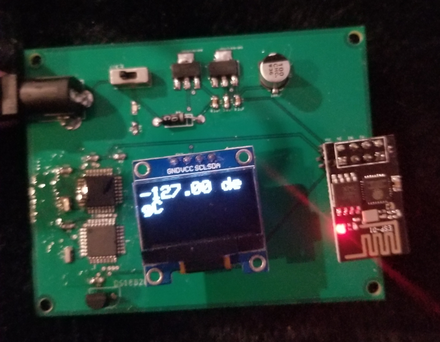
| DS18B20 Temperature Sensor |
1 |
| Adafruit SSD1306 OLED |
1 |
| ESP8266 WiFi Module |
1 |