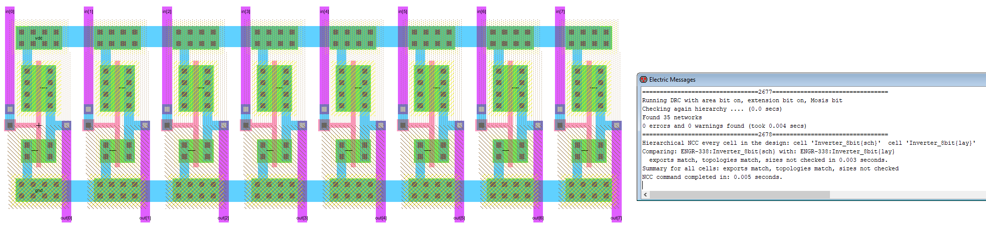
Figure 1 - Layout of the 8-bit Inverter w/ DRC and NCC checks passed
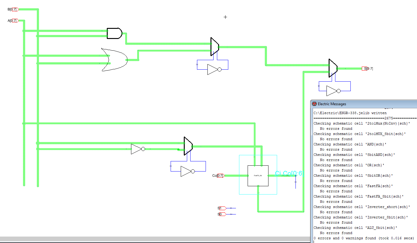
Figure 2 - Schematic of the 8-bit ALU with DRC checks passed.
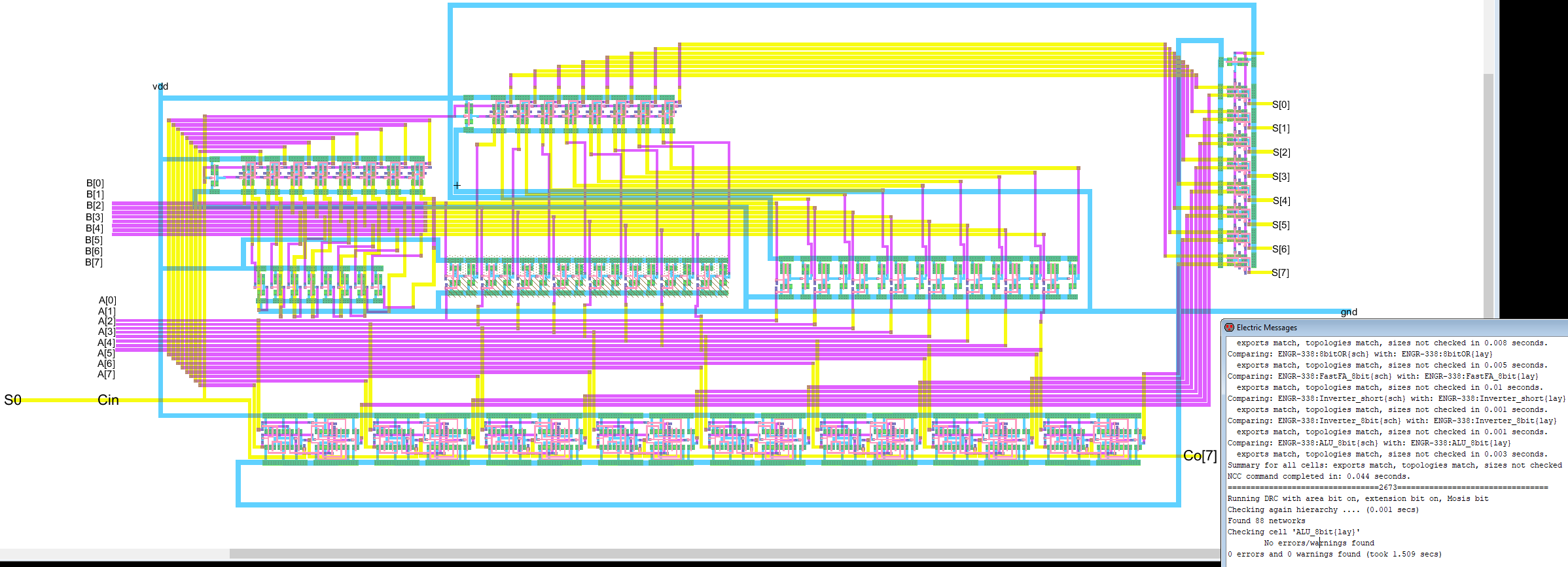
Figure 3 - Layout of the 8-bit ALU w/ DRC and NCC checks passed
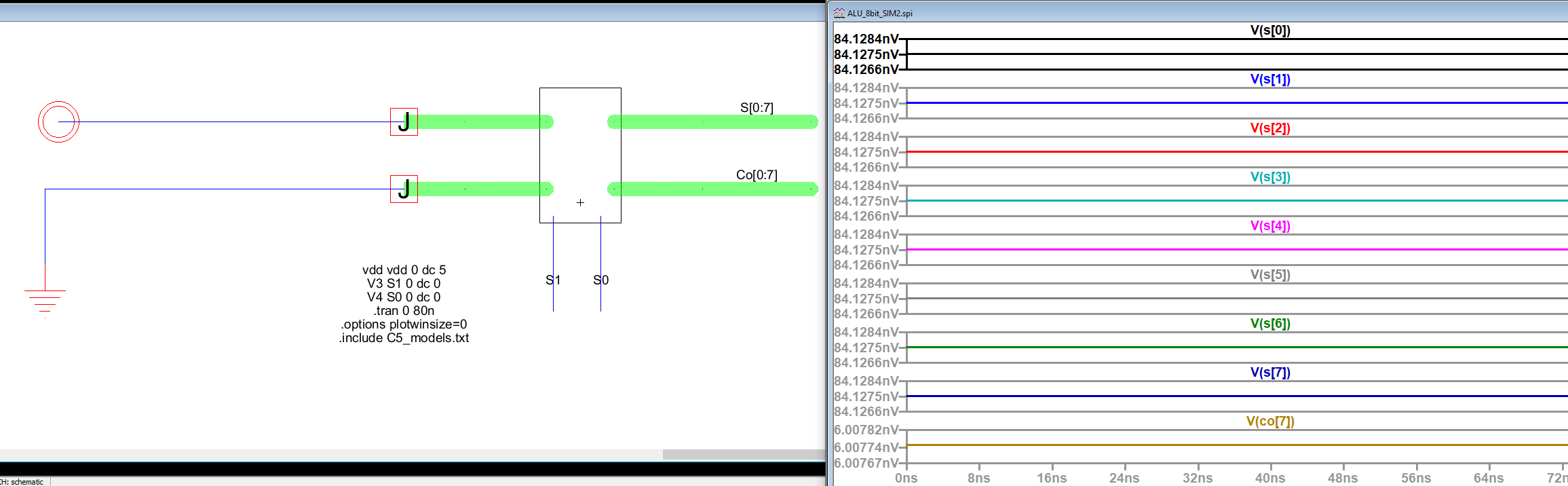
Figure 4 - Simulating AND logic showing all 0s for output as expected.
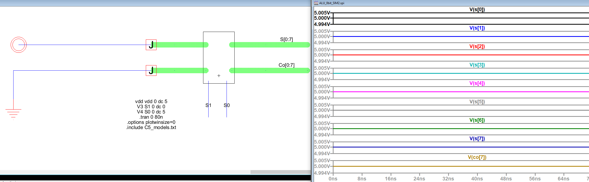
Figure 5 - Simulating OR logic showing all 1s for output as expected.
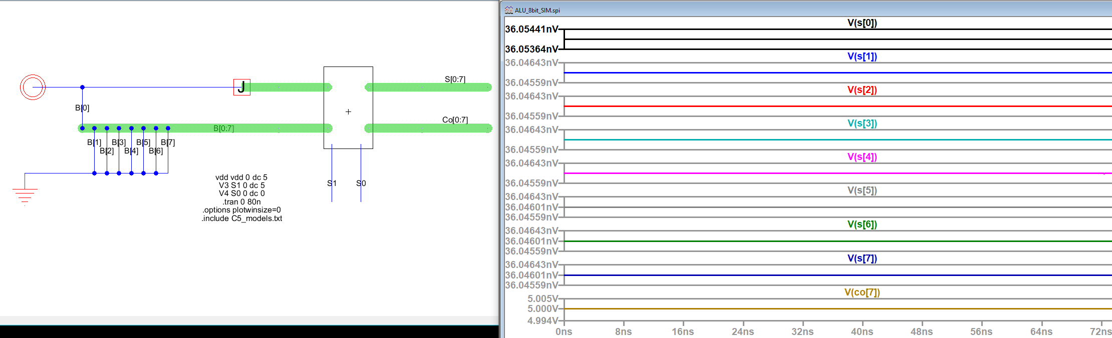
Figure 6 - Simulating addition operation for 0xFF + 0x01 with result S=0x00 and Co=1 as expected.
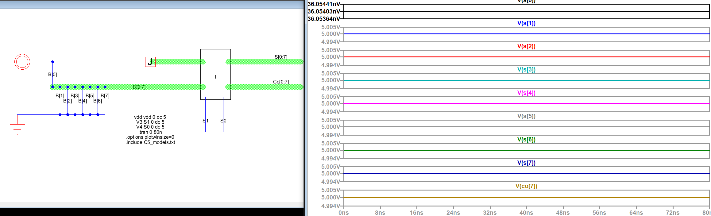
Figure 7 - Simulating subraction with 0xFF-0x01w/ S=0xFE, Co=0x01 as expected.
Discussion
Unlike previous labs the 8-bit ALU logic was verified after the layout was completed since I forgot to verify it first. However, as Figures 4 through 7 show, the 8-bit ALU is operating as it should. The layout itself was was created without much issue, it was just time consuming to make sure all the wires was neat and spaced properly.
Unlike previous labs the 8-bit ALU logic was verified after the layout was completed since I forgot to verify it first. However, as Figures 4 through 7 show, the 8-bit ALU is operating as it should. The layout itself was was created without much issue, it was just time consuming to make sure all the wires was neat and spaced properly.