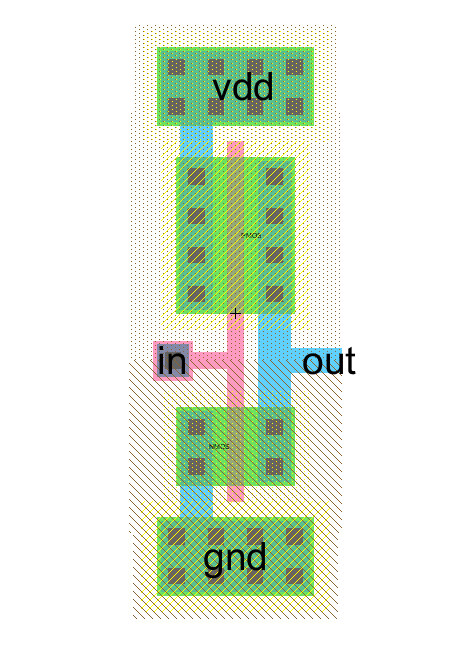
Figure 1 - Layout of the short inverter used for the ring oscillator
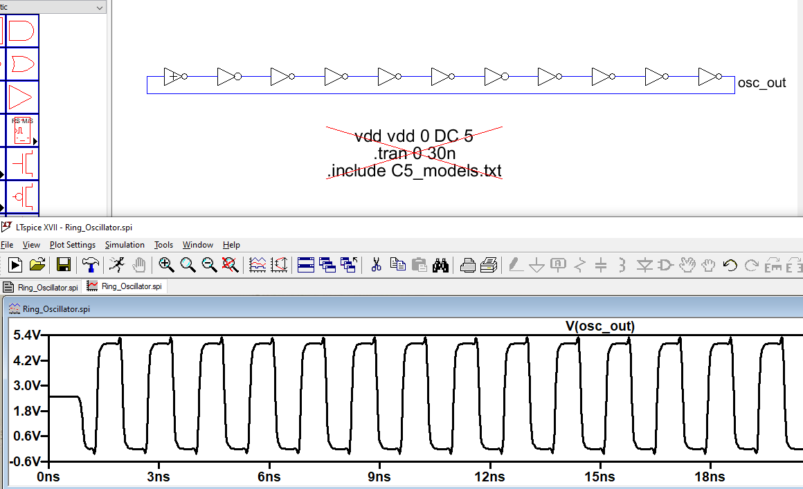
Figure 2 - Simulation of the ring oscillator without using buses
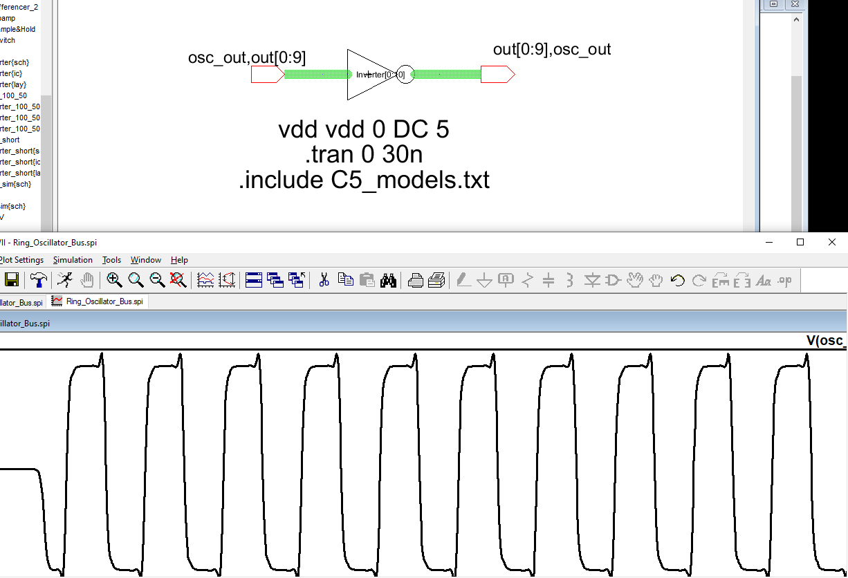
Figure 3 - Simulation of the ring oscillator using buses.
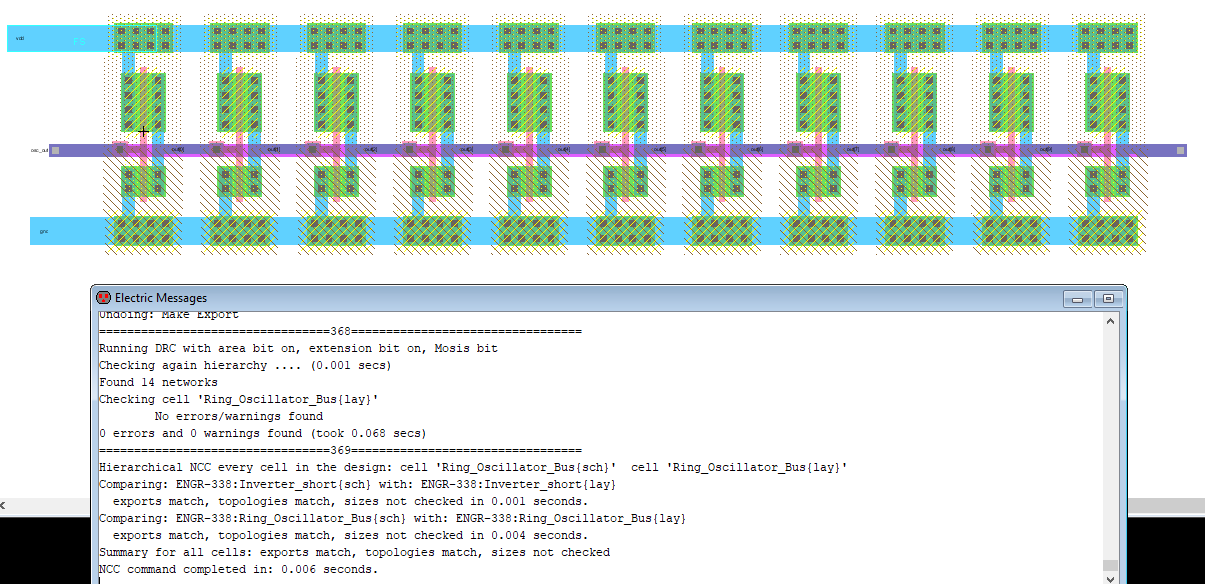
Figure 4 - Layout of the ring oscillator using short inverters.
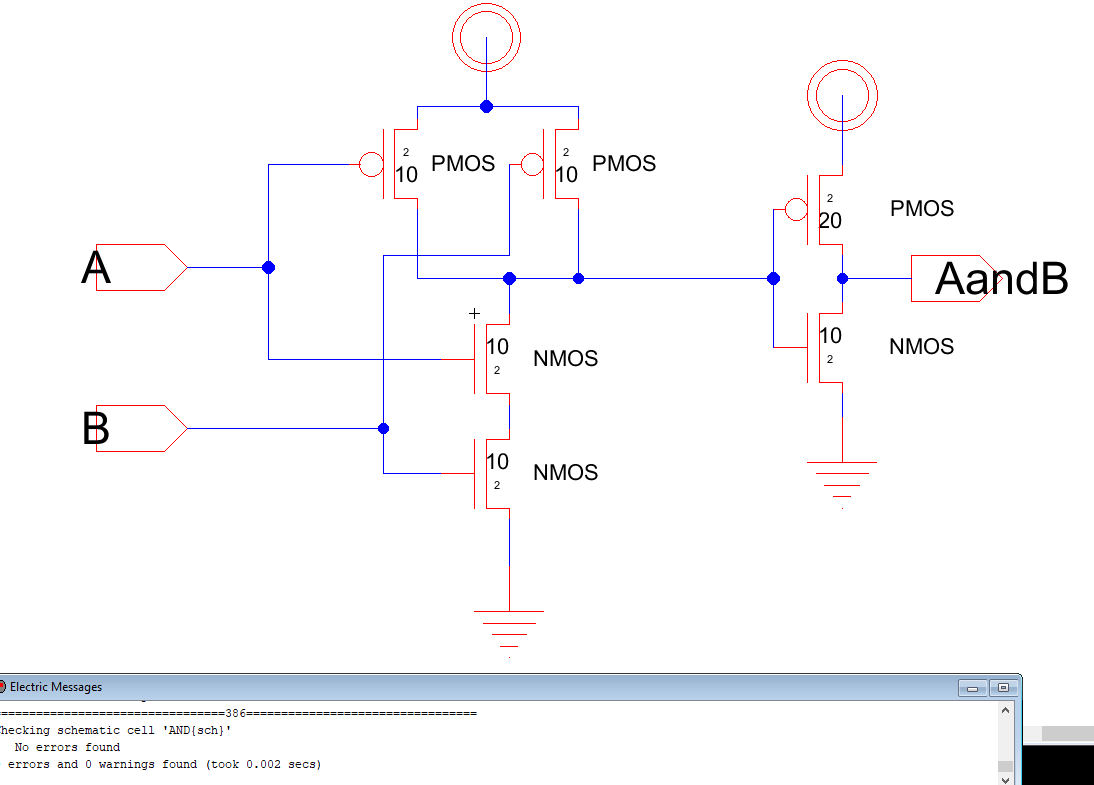
Figure 5 - Schematic for the AND gate
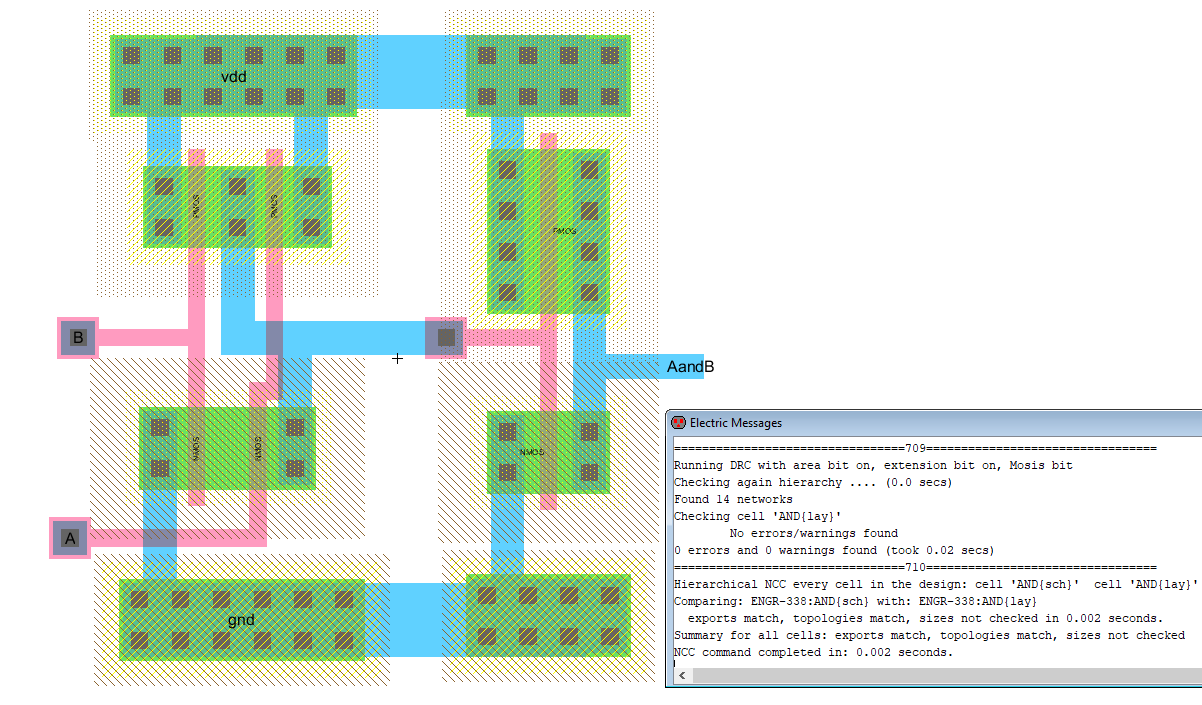
Figure 6 - Layout of AND gate
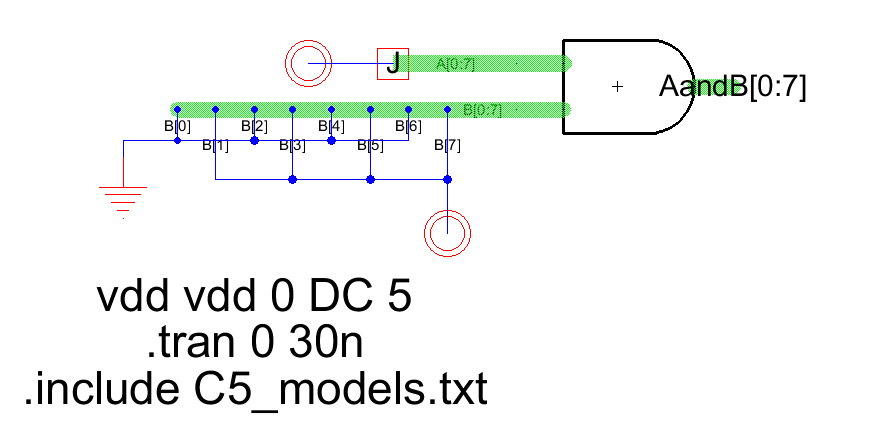
Figure 7 - Simulation schematic for the 8-bit AND
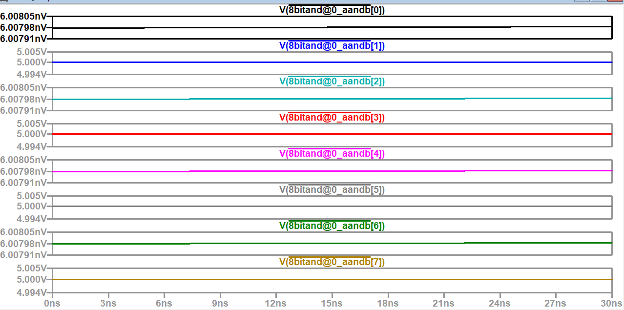
Figure 8 - Results for 8-bit AND simulation with A input at vdd
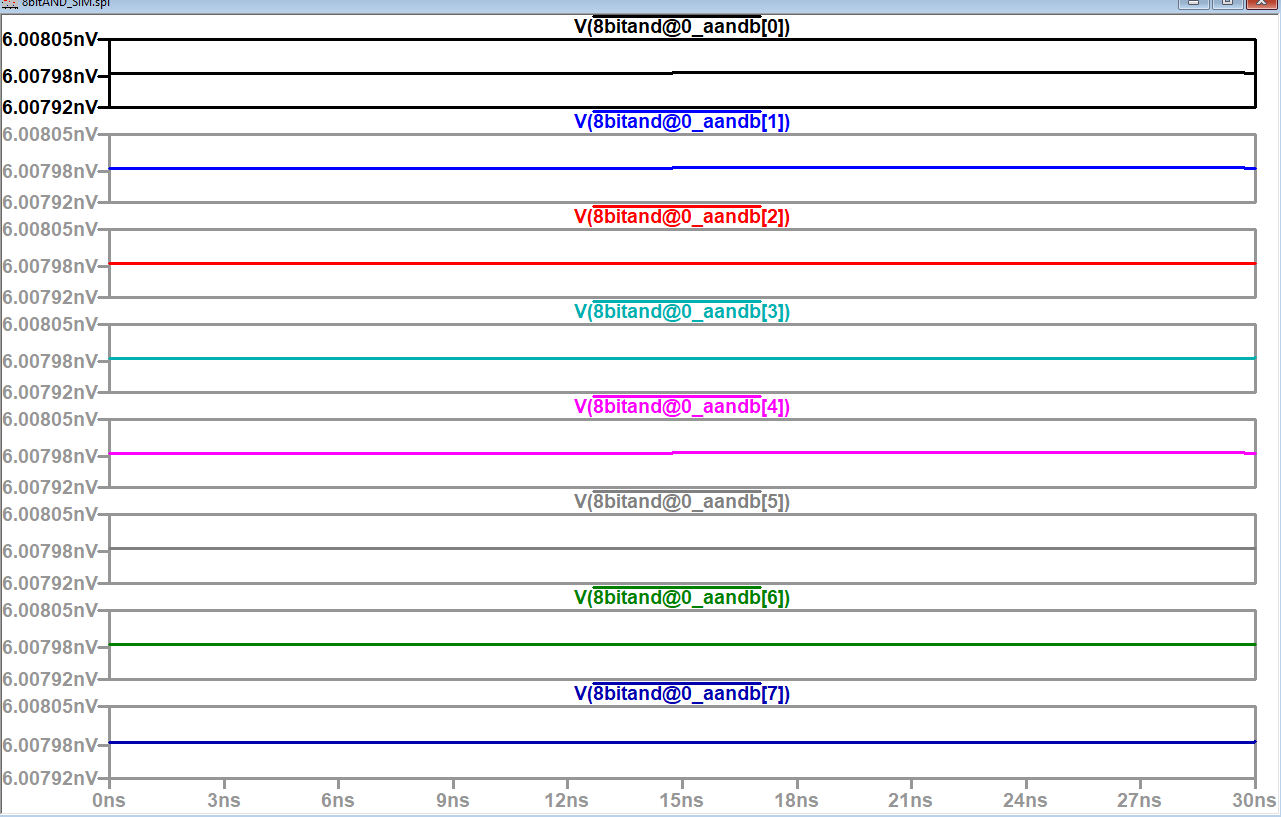
Figure 9 - Sim results for 8bit AND with A input grounded.
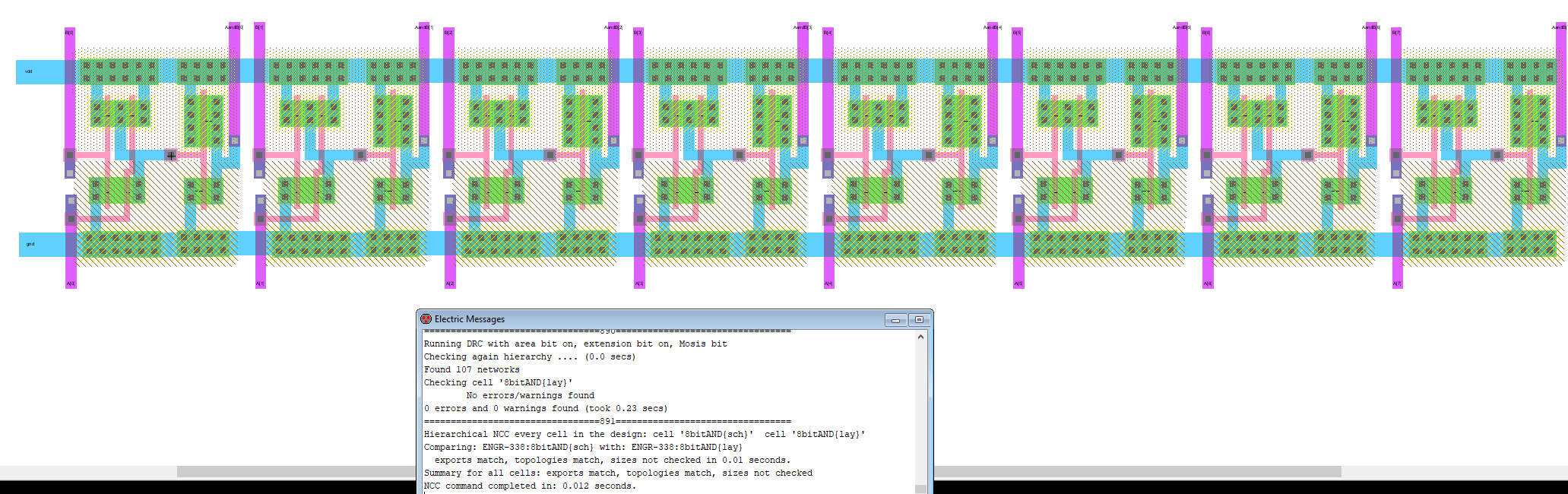
Figure 10 - Layout of the 8-bit AND gate.
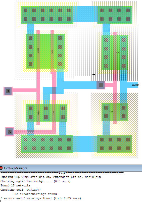
Figure 11 - Layout of the OR gate
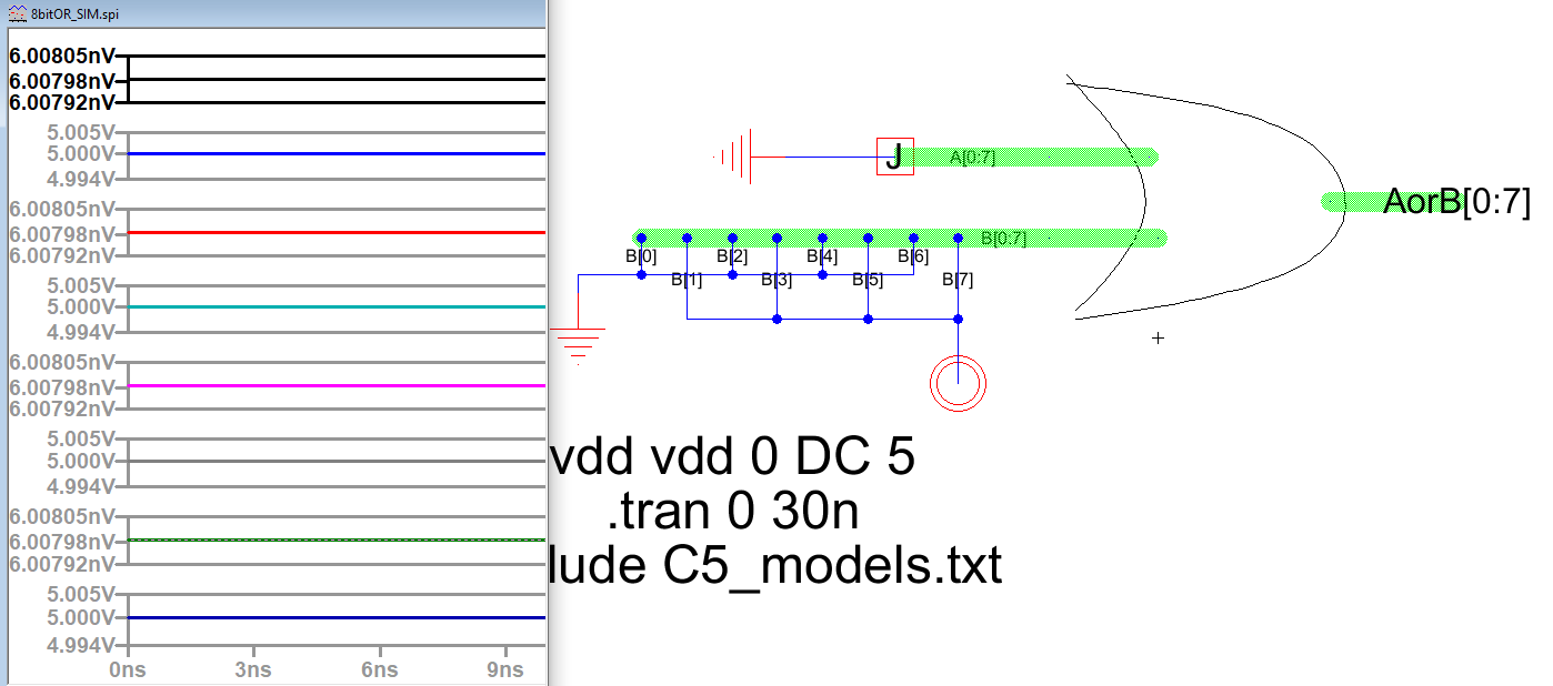
Figure 12 - Simulation of the 8-bit OR gate with input A grounded.
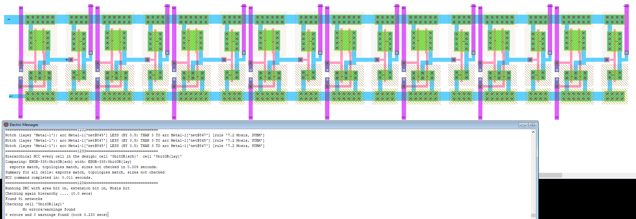
Figure 13 - Layout of the 8-bit OR gate.
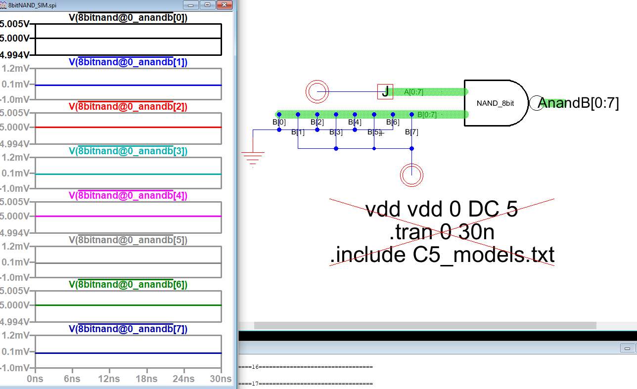
Figure 14 - 8bit NAND simulation with input A at vdd.
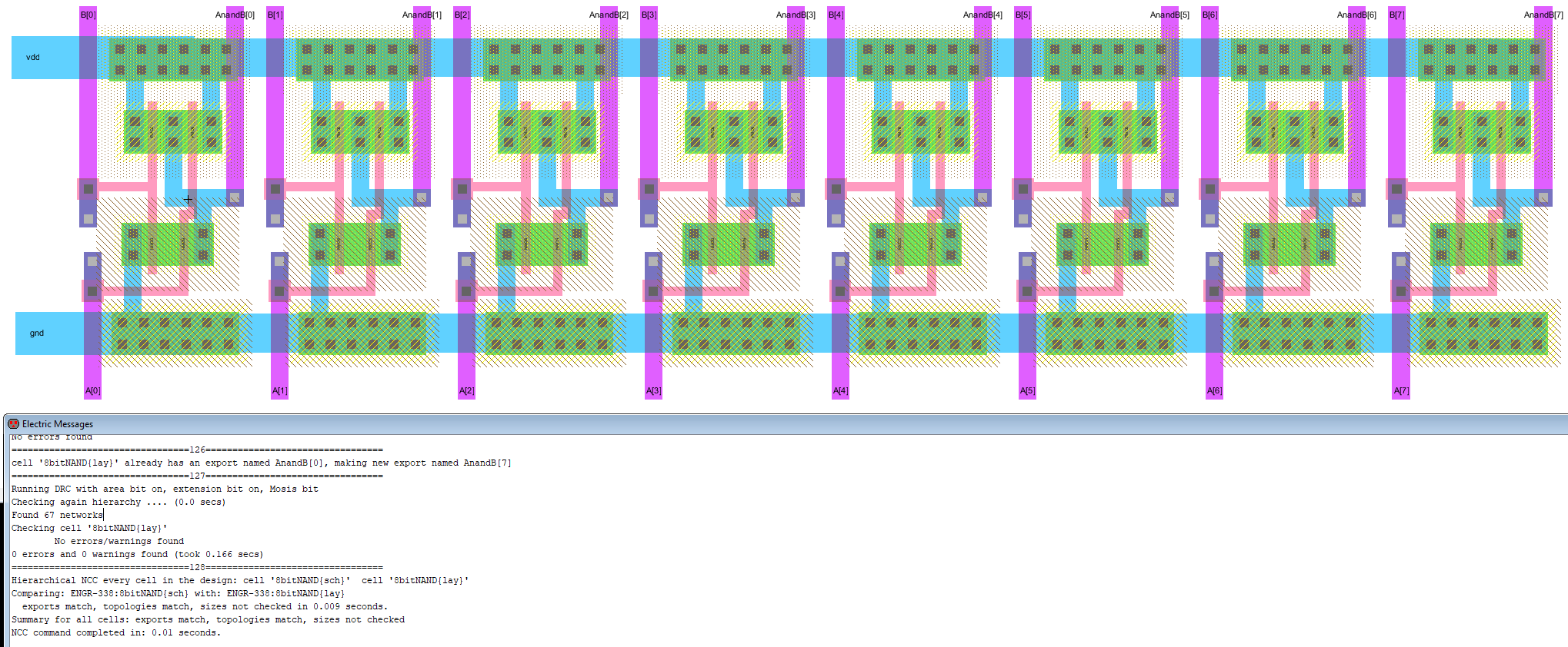
Figure 15 - Layout of the 8-bit NAND gate.
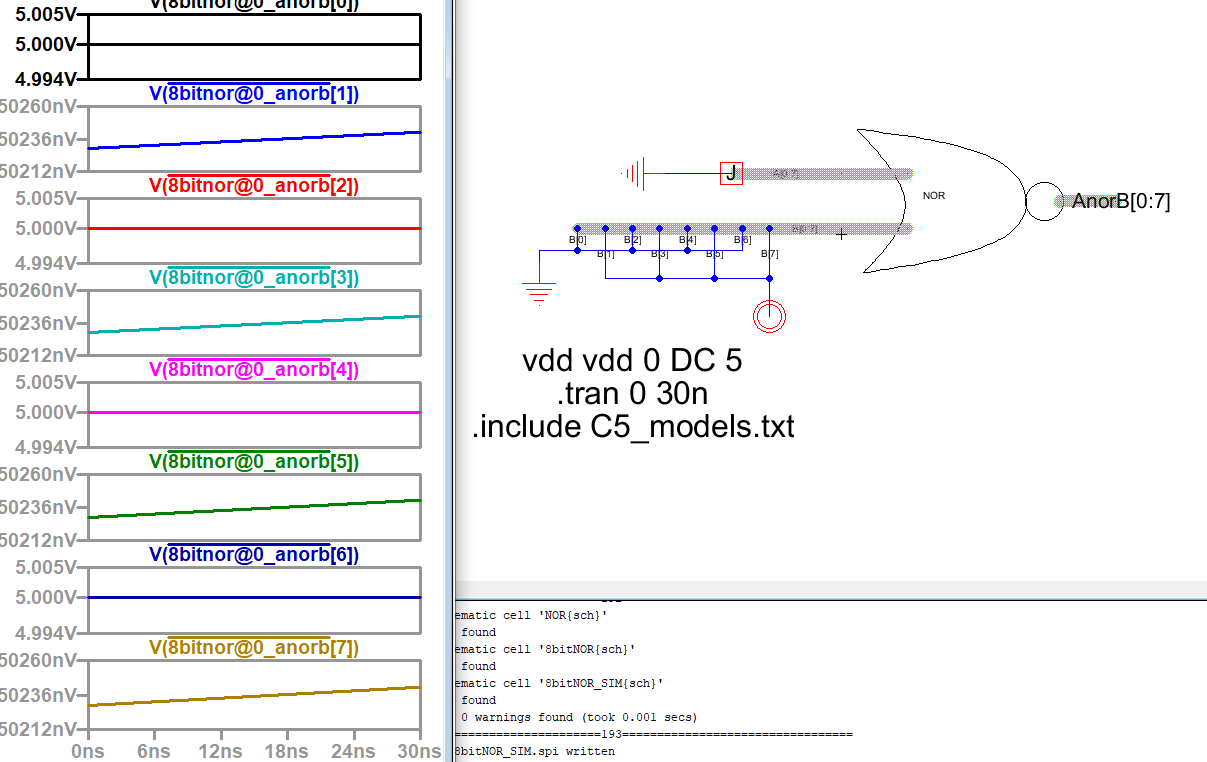
Figure 16 - Simulation of the 8-bit NOR gate with A input grounded.
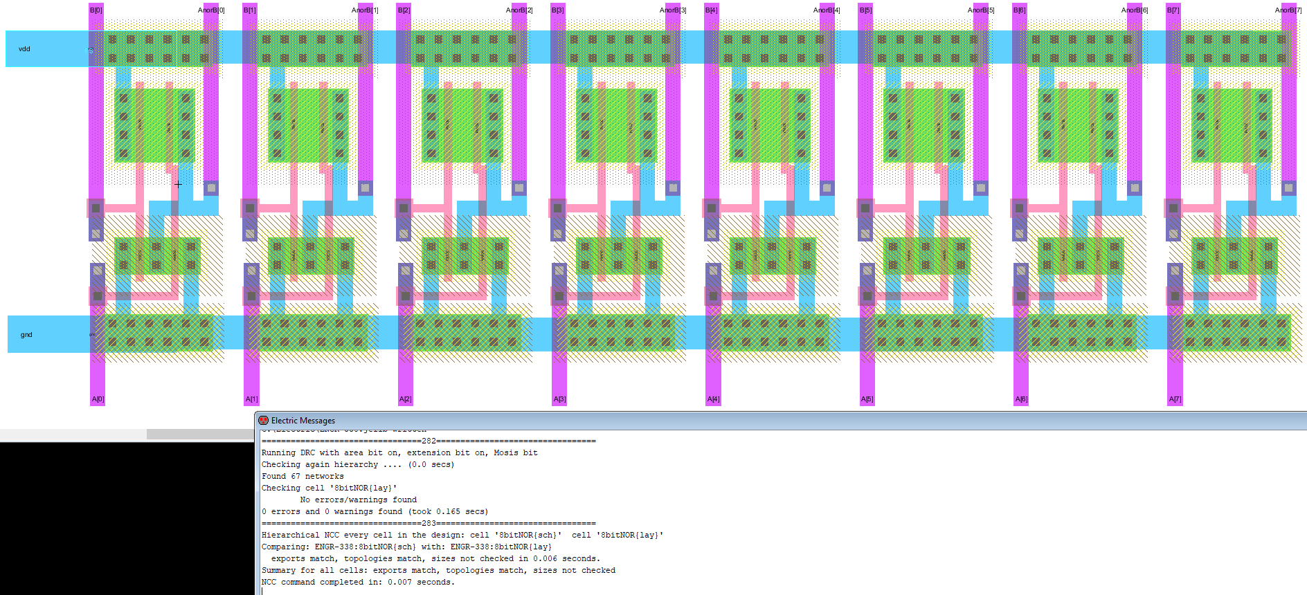
Figure 17 - Layout of the 8-bit NOR gate.
Discussion
The use of buses made the schematics very simple to create, read, and use. The layouts were all created by using the array function and then connecting the vdd/gnd rails and creating all the exports, which made the layout creations pretty quick and straightforward after minor adjustments were made to the original 1-bit gates. The layouts do not use buses because CMOS has severe limitations on current output, so having multiple TTL devices connected to the same bus will likely not function well.
The use of buses made the schematics very simple to create, read, and use. The layouts were all created by using the array function and then connecting the vdd/gnd rails and creating all the exports, which made the layout creations pretty quick and straightforward after minor adjustments were made to the original 1-bit gates. The layouts do not use buses because CMOS has severe limitations on current output, so having multiple TTL devices connected to the same bus will likely not function well.