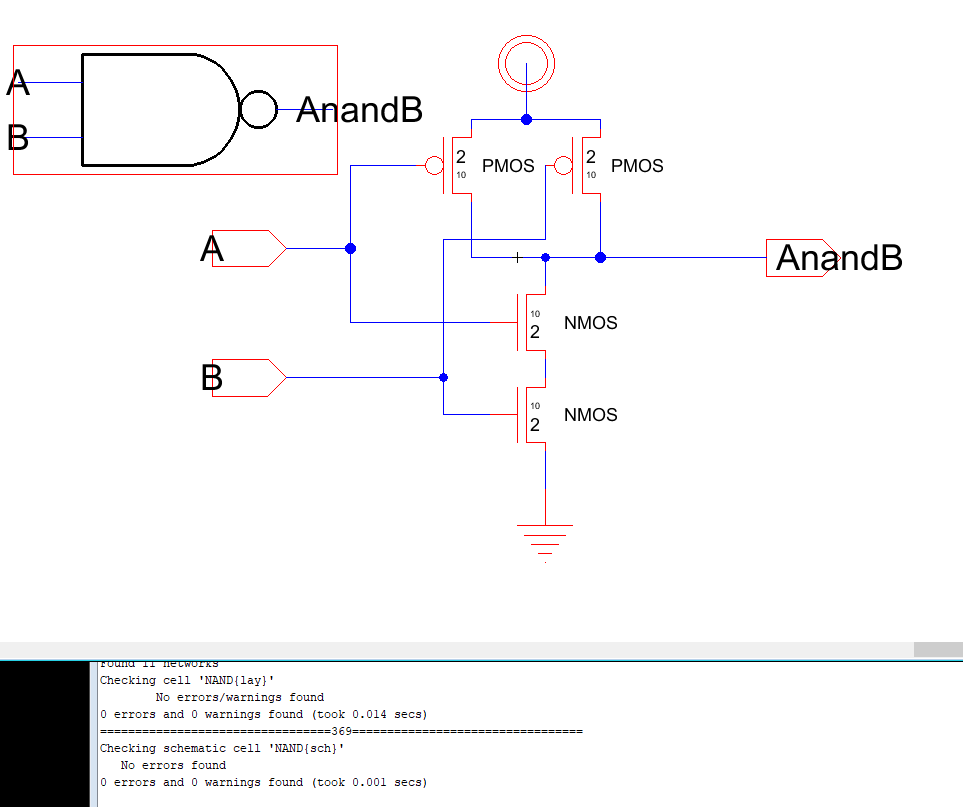
Figure 1 - Schematic of the NAND gate.
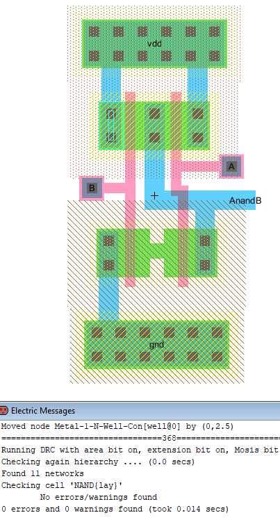
Figure 2 - Layout of the NAND gate.
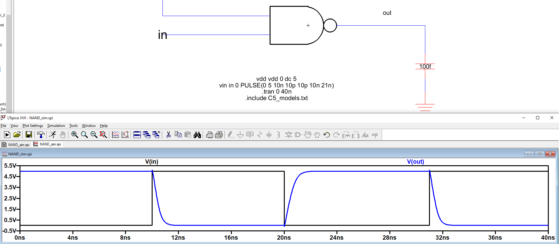
Figure 3 - Simulation of the NAND gate driving a 100fF capacitor
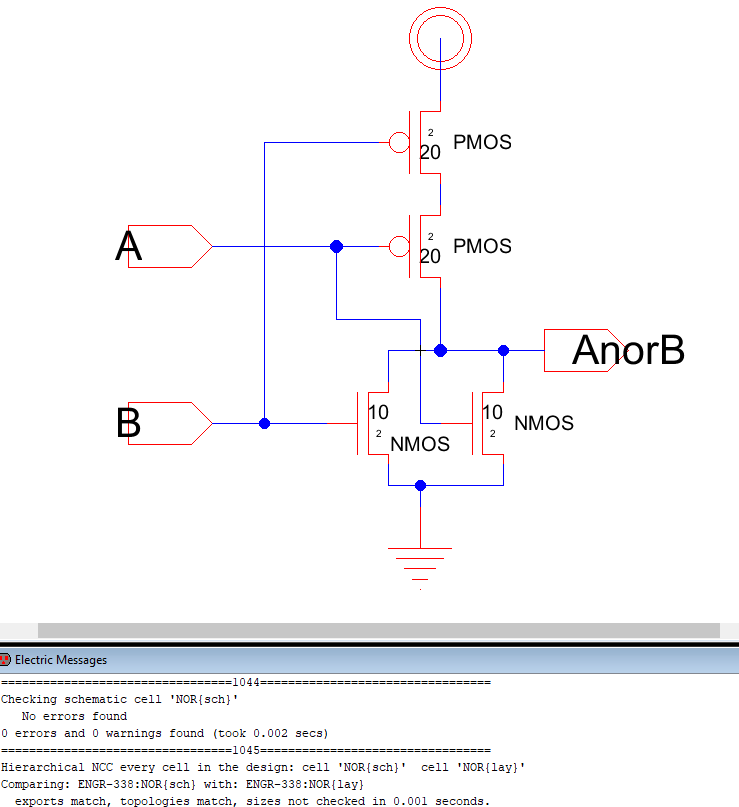
Figure 4 - Schematic of the NOR gate
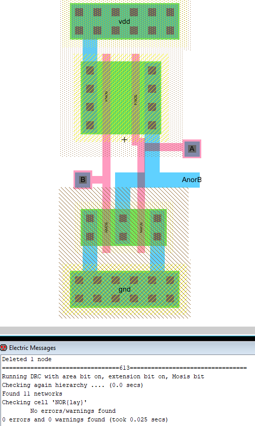
Figure 5 - Layout of the NOR gate
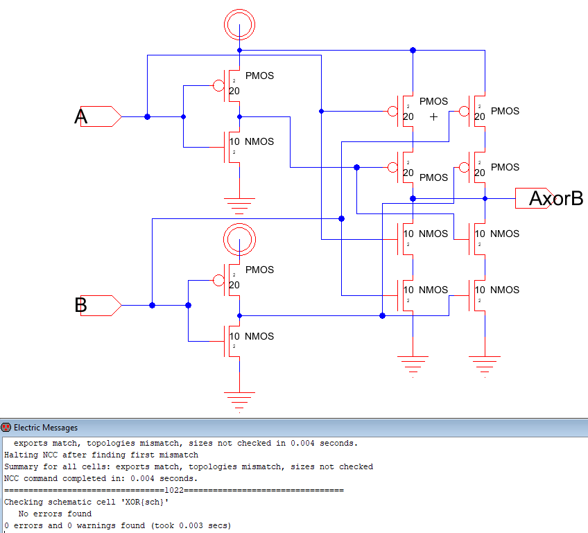
Figure 6 - Schematic of the XOR gate.
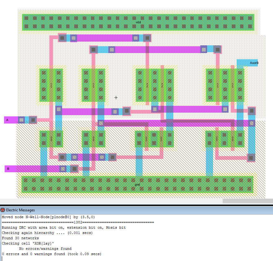
Figure 7 - Layout of the XOR gate. Passes the DRC as shown, but fails the NCC check.
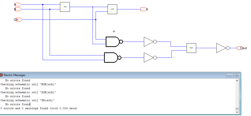
Figure 8 - Schematic of the full adder. The XOR and NOR gates are labeled boxes instead of their appropriate symbols.
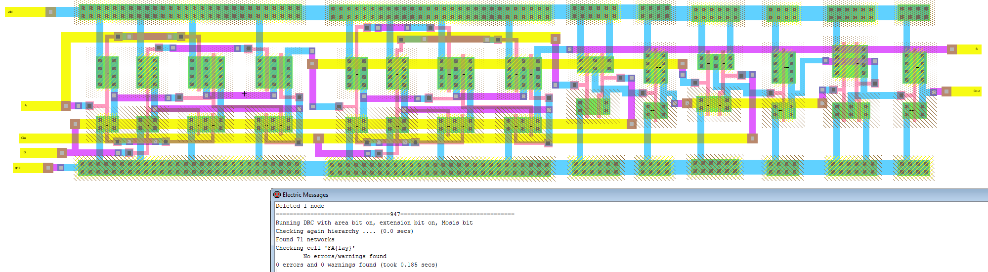
Figure 9 - Full Adder layout.
Discussion
For the most part, the designs were made without too much hassle. There are a few problems overall. First, I couldn't figure out how you're supposed to be able to free-draw in ElectricVLSI. Secondly, while the XOR gate passes the DRC check, it fails the NCC check. For some reason the NCC checker is not able to recognize the PMOS transistors in the schematic as the PMOS transistors in the layout. These were remade, rewired, and set as spice models(again), but the NCC check is still failing for some reason. The NCC check passes for all other designs, however. In the Full Adder schematic, the two XOR segments are slightly different with the A and B PMOS gate connections as for some reason the DRC check failed on one but not the other only when the vdd wells were connected. The DRC check and well check passes on the Full Adder after the fix. Because the XOR gate fails the NCC check, the Full Adder fails the NCC check because of the problems with the PMOS transistors that I have not been able to solve.
For the most part, the designs were made without too much hassle. There are a few problems overall. First, I couldn't figure out how you're supposed to be able to free-draw in ElectricVLSI. Secondly, while the XOR gate passes the DRC check, it fails the NCC check. For some reason the NCC checker is not able to recognize the PMOS transistors in the schematic as the PMOS transistors in the layout. These were remade, rewired, and set as spice models(again), but the NCC check is still failing for some reason. The NCC check passes for all other designs, however. In the Full Adder schematic, the two XOR segments are slightly different with the A and B PMOS gate connections as for some reason the DRC check failed on one but not the other only when the vdd wells were connected. The DRC check and well check passes on the Full Adder after the fix. Because the XOR gate fails the NCC check, the Full Adder fails the NCC check because of the problems with the PMOS transistors that I have not been able to solve.