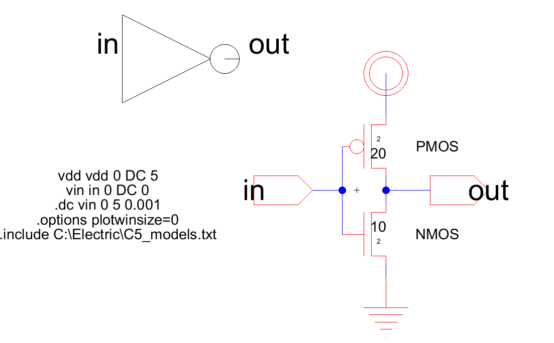
Figure 1 - Schematic of the 20/10 inverter
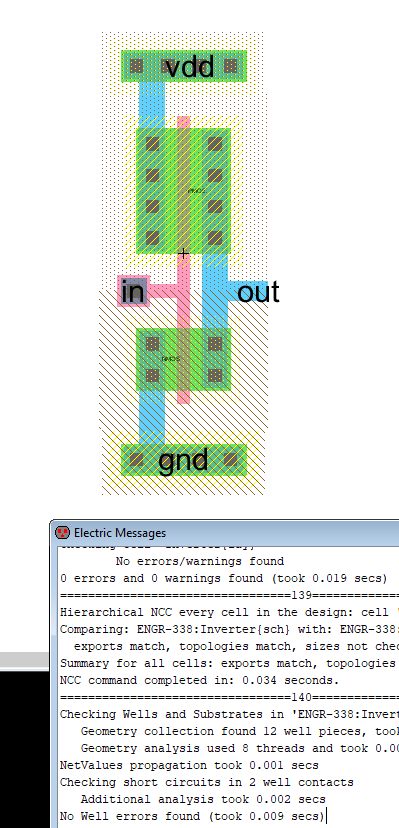
Figure 2 - Layout of inverter with passed checks.
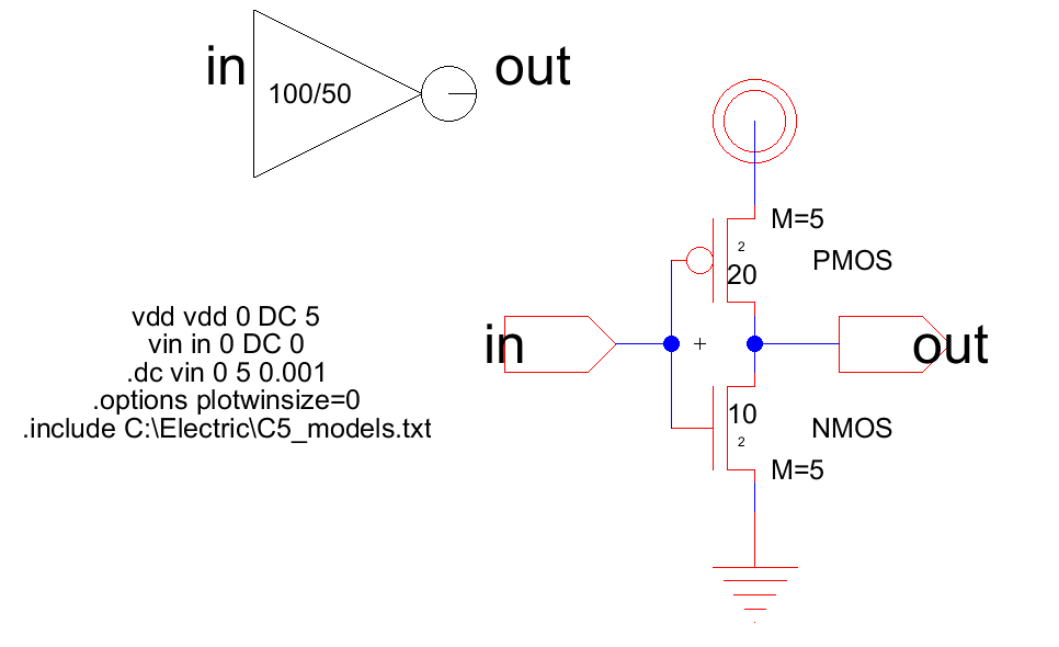
Figure 3 - 100/50 schematic
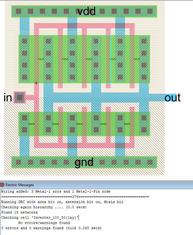
Figure 4 - Layout of the 100/50 inverter with passed DRC checks.
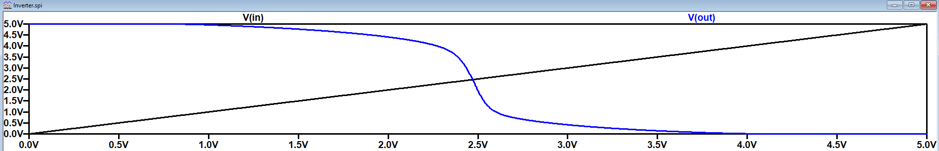
Figure 5 - Test simulation of the inverter.
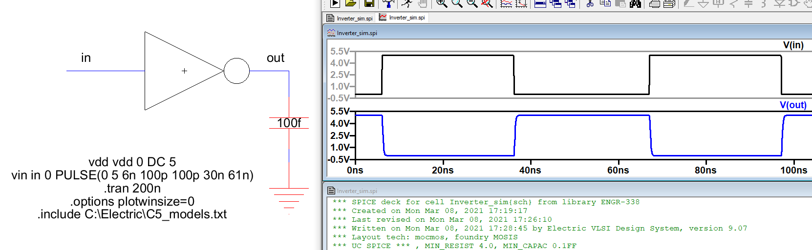
Figure 6 - Simulating the 20/10 inverter driving a 100fF load
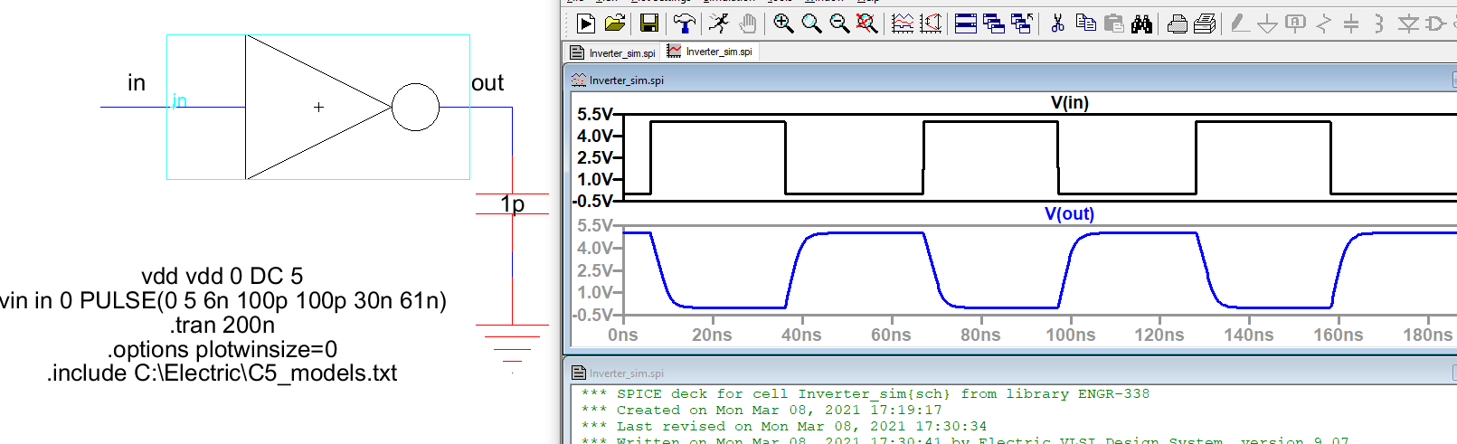
Figure 7 - Simulating the 20/10 inverter driving a 1pF load
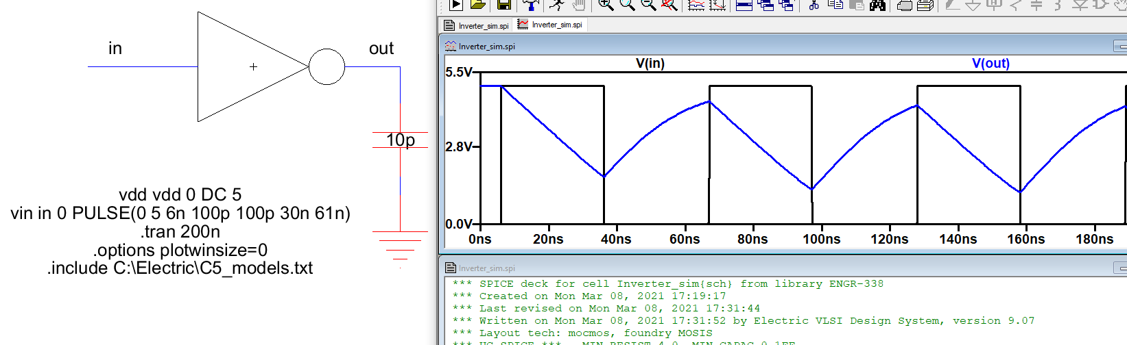
Figure 8 - Simulating the 20/10 inverter driving a 10pF load. The inverter is unable to drive the 10pF load.
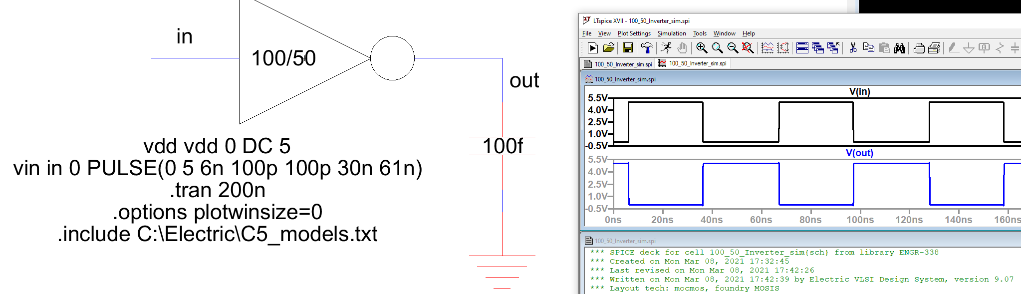
Figure 9 - Simulating the 100/50 inverter driving the 100fF load.
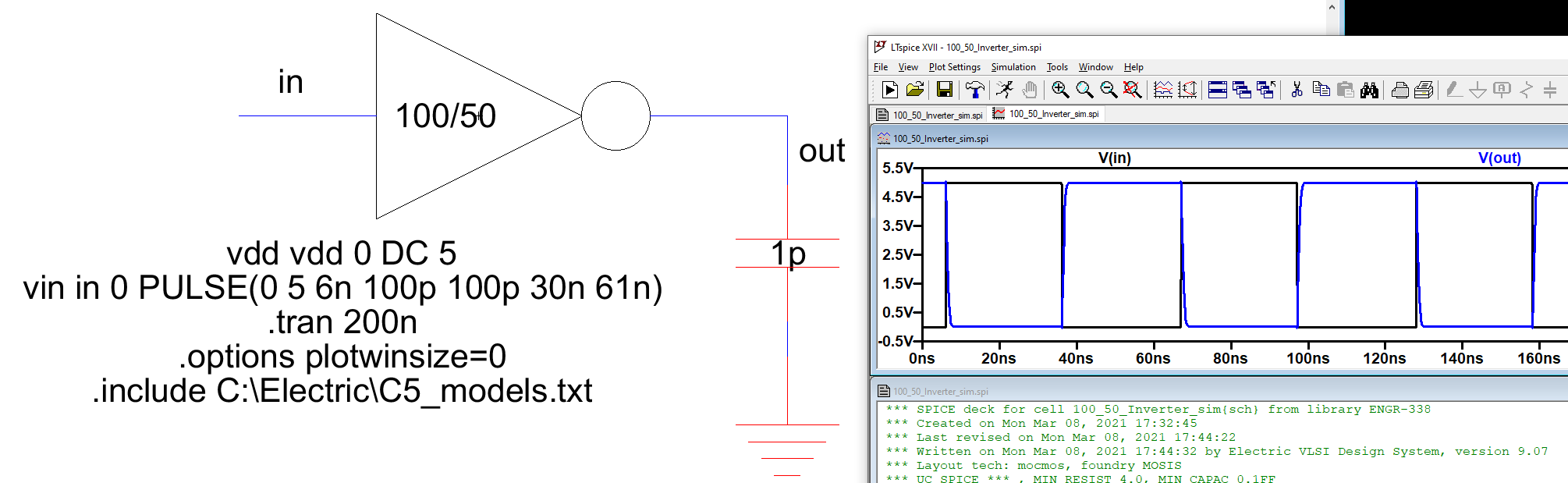
Figure 10 - Simulating the 100/50 inverter driving the 1pF load, showing some slight time delay.
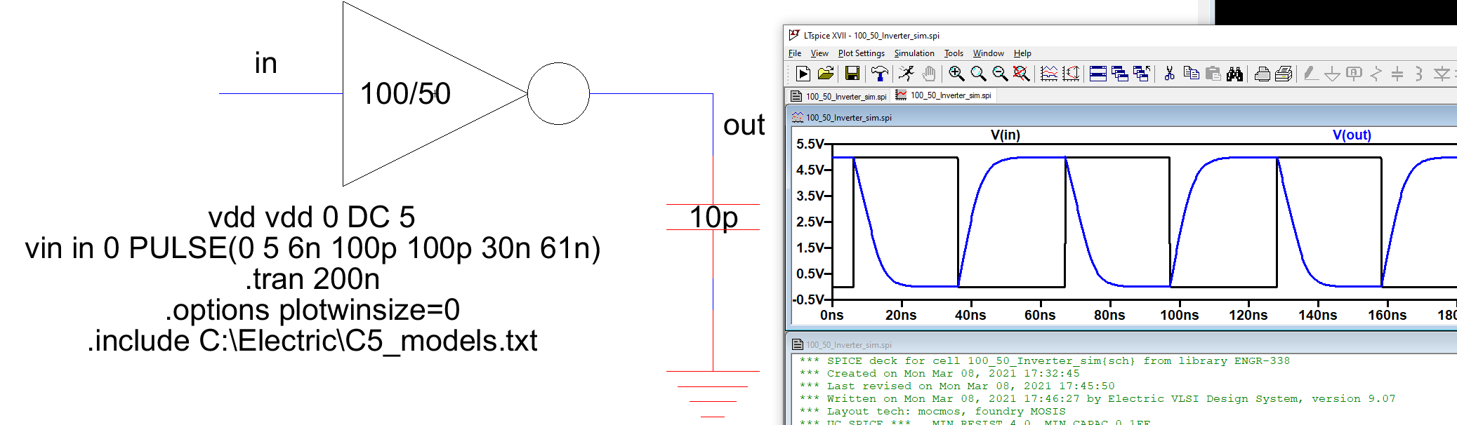
Figure 11 - Simulating the 100/50 inverter driving the 10pF load, with more prevalent delay shown.
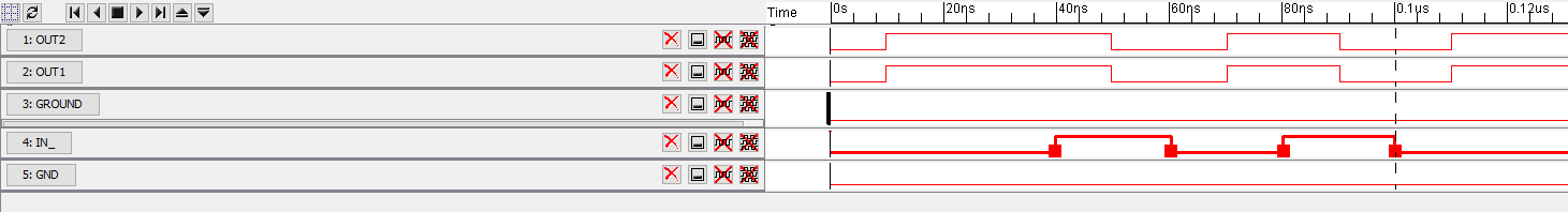
Figure 12 - ALS simulation showing the time delays of both the outputs.
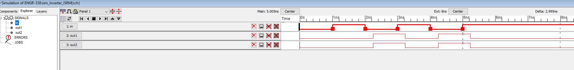
Figure 13 - ISRM simulation showing the time delay with both voltage outputs.
Discussion
The schematics and layouts were built without any problems. The interesting thing with the simulations using the ALS and ISRM tools is that the ALS simulation showed an approximate 10ns time delay when the input voltage switched to high, while the ISRM tool showed a 0.1ns time delay when the input voltage switched to high.
The schematics and layouts were built without any problems. The interesting thing with the simulations using the ALS and ISRM tools is that the ALS simulation showed an approximate 10ns time delay when the input voltage switched to high, while the ISRM tool showed a 0.1ns time delay when the input voltage switched to high.