CE 338 2021 Spring
Lab 9: Design a Simple 8-Bit ALU
Nic Theobald
nstheobald@fortlewis.edu
Simple 8-bit ALU
Introduction
This
lab covers the design and simulation of an 8-bit ALU.
Methods and Materials
Item
Quantity
LTspice
Electric VLSI
Ideal ADC/DAC Library
1
1
1
The schematic of the ALU was created and simulated using
LTspice. All 4 modes were tested and verified. The layout was then
created and verified using DRC, NCC, and ERC.
Results
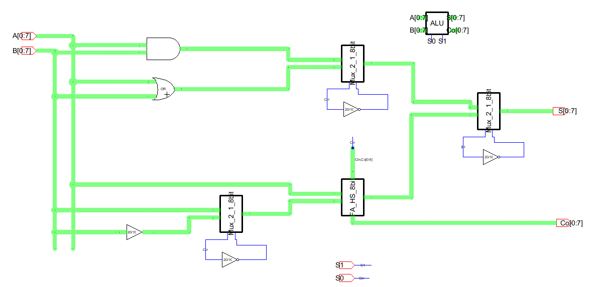
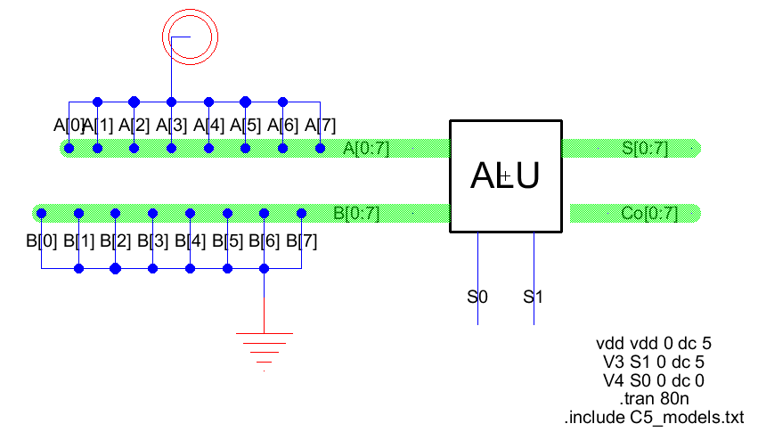
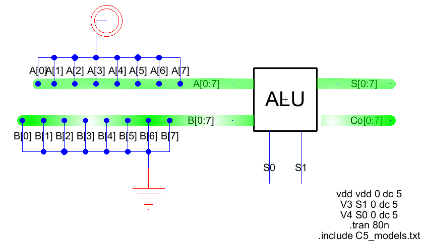
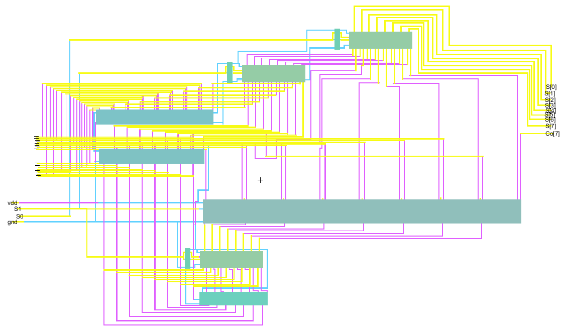
Task 1: Create Schematic The schematic for the ALU was first created.
Figure
1: Schematic view of the 8-bit ALU.
An 8-bit inverted was also created, along with the layout.
Figure 2: 8-bit inverter schematic.
Figure 3: Layout of 8-bit inverter.
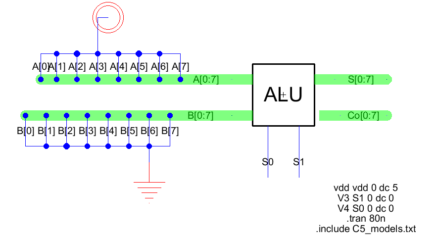
It was then simulated in LTspice.
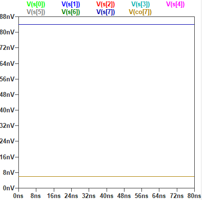
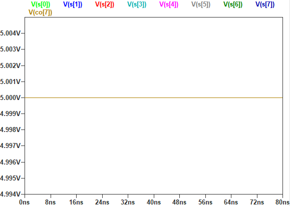
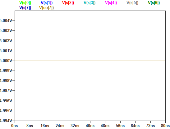
AND
Figure 4:Simulation 11111111 and 00000000
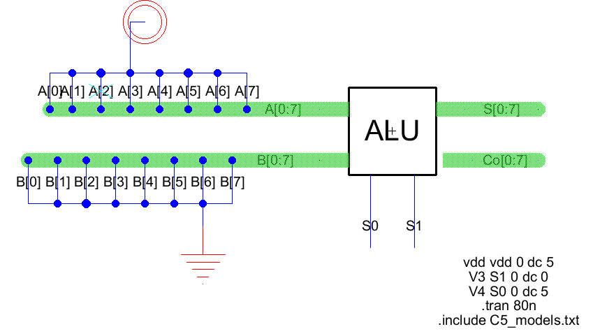
OR
Figure 5:Simulation 11111111 OR 00000000
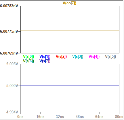
ADD
Figure 4:Simulation 11111111 + 00000000
Subtract
Figure 5: Simulation 11111111 - 00000000
Task 2: Create and Verify Layout
The layout of the ALU was created.
Figure 5: ALU Layout.
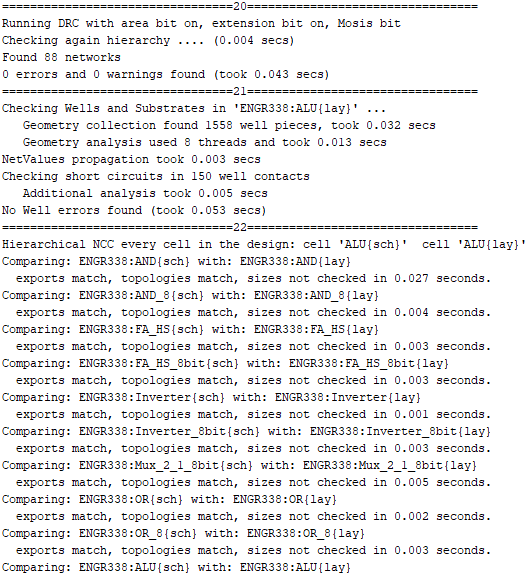
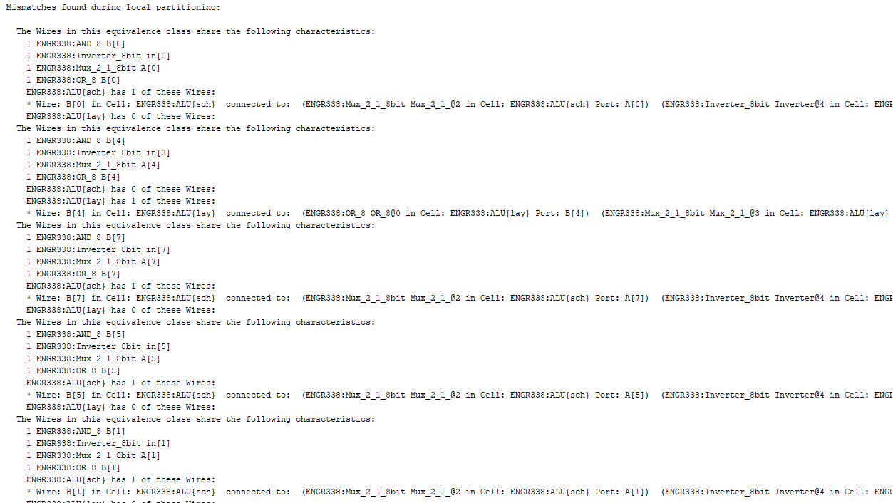
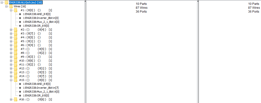
DRC, ERC, and NCC was run. NCC failed...
continued...
Figure 6: DRC, ERC, NCC check.
Discussion:
This lab detailed the design and simulation of an 8 bit ALU. All verification methods, other than NCC, passed.