CE 338 2021 Spring
Lab 8: MUX and High-Speed Full Adder
Nic Theobald
nstheobald@fortlewis.edu
MUX and High-Speed Full Adder
Introduction
This
lab covers the design and simulation a MUX and High-Speed Full Adder.
Methods and Materials
|
|
Item
|
Quantity
|
|
|
LTspice
Electric VLSI
Ideal ADC/DAC Library
|
1
1
1
|
|
|
Schematics and layout views were created for the MUX and High speed full adder. 8-bit versions were also created.
Results
Task 1: Build and Simulate a Ring Oscillator
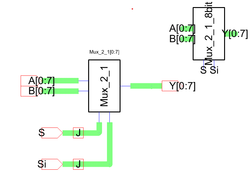
The schematic for both 8-bit muxs were created.
Figure
1: Schematic view of the 8-bit mux.
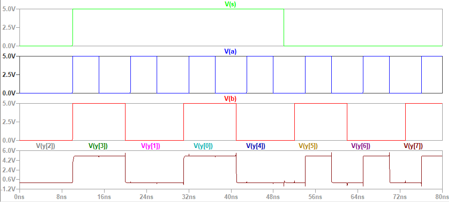
It was then simulated in LTspice.
Figure
2:Simulation of 8-bit mux.
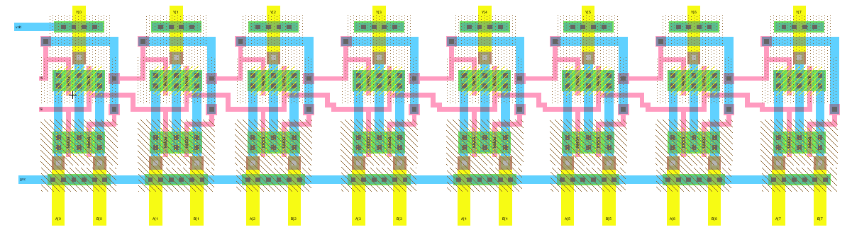
The layout of the 8-bit mux was then created.
Figure 3: Layout view of the 8-bit mux.
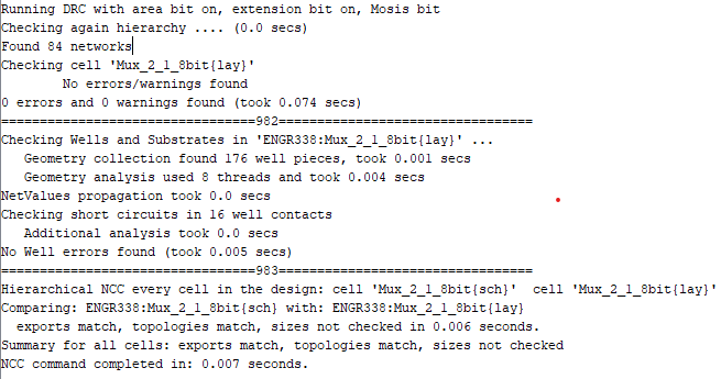
ERC, DRC, and NCC were also checked.
Figure 4: Checking for errors.
Task 2: Design an 1-bit high speed adder
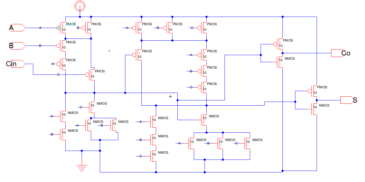
The schematic of the 1-bit high speed adder was first created and simulated
Figure 5: Schematic view of the 1-bit high speed adder.
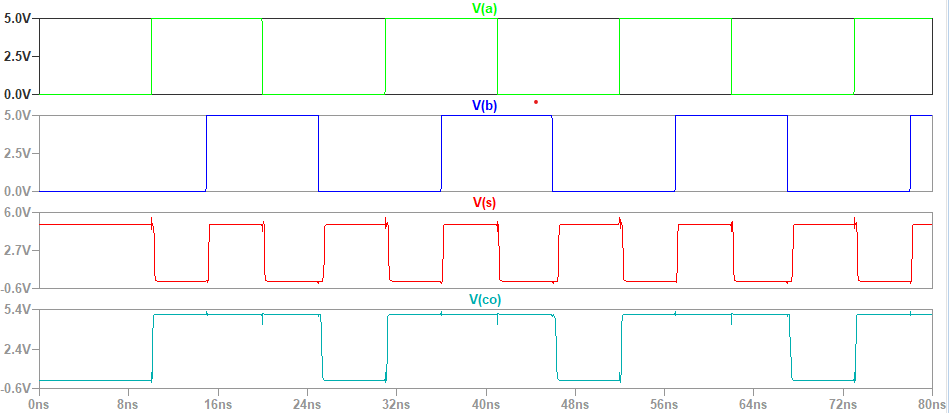
The schematic was then simulated in LTspice.
Figure 6:Simulation on 1-bit high speed adder.
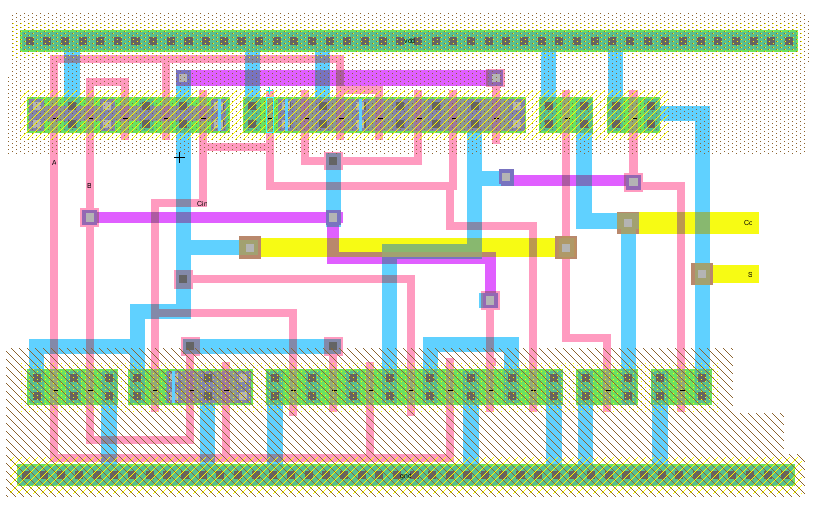
The layout of the 1-bit high speed adder was then created.
Figure 7: Layout view of the 1-bit high speed adder.
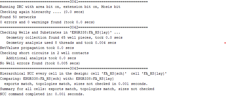
ERC, DRC, and NCC were also checked.
Figure 8: Checking for errors.
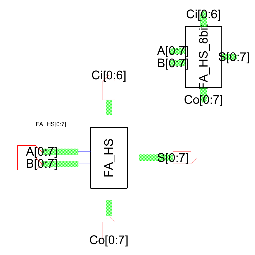
Task 3: Design 8-bit High Speed Adder
The schematic of the 8 bit adder was first created and simulated
Figure 5: Schematic view of the 8 bit adder.
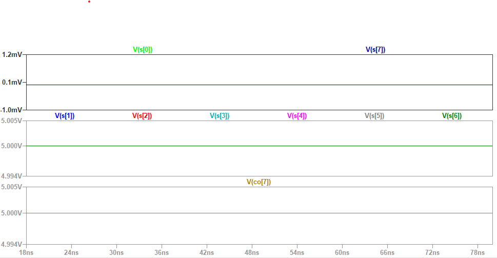
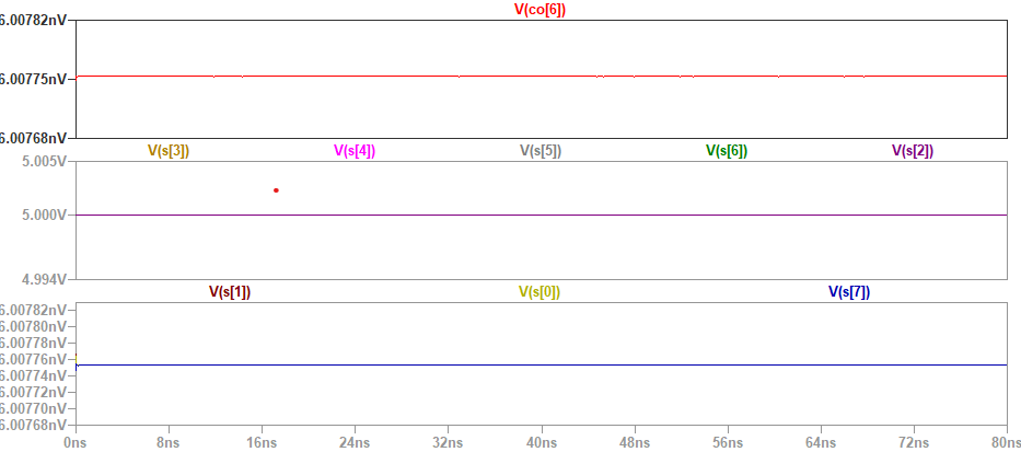
The schematic was then simulated in LTspice.
Figure
2:Simulation on 8 bit adder.
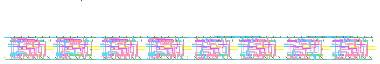
The layout of the 8 bit adder was then created.
Figure 3: Layout view of the 8 bit adder.
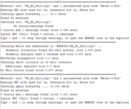
ERC, DRC, and NCC were also checked.
Figure 4: Checking for errors.
Discussion:
This lab detailed the design and simulation of an 8 bit MUX and and 8 bit Adder.