CE 338 2021 Spring
Lab 2: Layout of R-2R DAC
Nic Theobald
nstheobald@fortlewis.edu


R-2R DAC Layout

Introduction

This lab covers the layout and simulation of an R-2R DAC. Electric VLSI is used in the layout of the DAC, through the use of an n-well resistor ladder. The design was then verified using LTspice.

Methods and Materials


Item
Quantity


LTspice
Electric VLSI
Ideal ADC/DAC Library
1
1
1


The resistor ladder was first simplified into several sub cells (Figure 1). These sub cells were then used to form the full ladder (Figure 2). The sub cell was formed into a layout (Figure 3) which was then formed into the full resistor ladder (Figure 4).  DRC and NCC checks were run to confirm layout-schematic continuity and that the design is error free (Figure 5, 6). The design was simulated (Figure 7).

Results

Task 1: Create Schematic for Resistor Ladder

The resistor branch was simplified into the following R-2R sub cell.


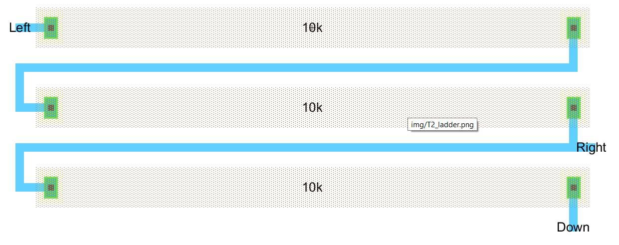
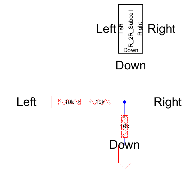
Figure 1: Schematic view of the R-2R sub cell.

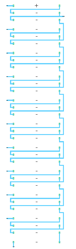
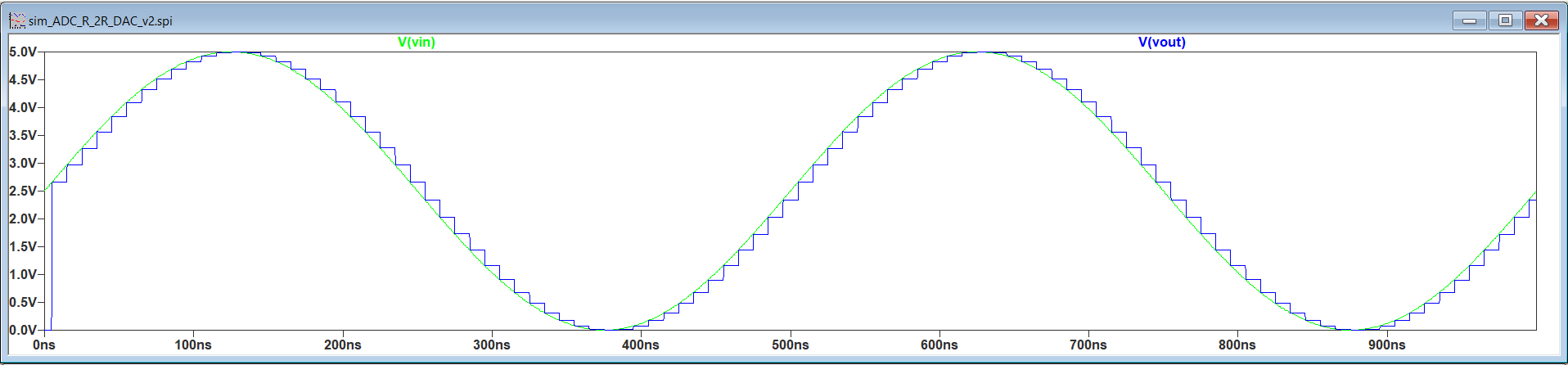
The resistor ladder was simplified into the following, using the R-2R sub cell.


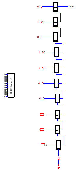
Figure 2: Schematic view of the R-2R ladder composed of the sub cells.


Task 2: Create Layout for Resistor Ladder

The sub cell layout was first created and converted to an icon.


Figure 3: Sub cell layout.
Using the sub cell icon, the full ladder was layed out.


Figure 4: Layout of resistor ladder.

A DRC and NCC Check was run.


Figure 5: DRC check.


Figure 6: NCC check.


The schematic was then simulated using the ideal ADC.


Figure 7: Design simulation.


Discussion:

The layout and schematic of the DAC was simplified into sub cells. These sub cells were used to form the larger R-2R ladder that forms the DAC. DRC and NCC checks were performed to ensure that the design was error free and consistent. The design was then simulated to ensure that it functions correctly.