CE 338 2021 Spring
Lab 2: Design of R-2R DAC
Nic Theobald
nstheobald@fortlewis.edu


R-2R DAC Design

Introduction

This lab covers the design and simulation of an R-2R DAC. Electric VLSI is used in the design of the DAC, through the use of an n-well resistor ladder. The design was then verified using LTspice. The design was also compared to a prebuild ideal DAC.

Methods and Materials


Item
Quantity


LTspice
Electric VLSI
Ideal ADC/DAC Library
1
1
1


This lab assumes that LTspice and ElectricVLSI are already installed and set up. The library containing the ideal ADC and DAC were installed and copied into a new library. The ADC/DAC combination was opened and simulated in LTspice (Figure 1). Figure 2 shows the results of the ADC/DAC simulation. The steps of the DAC output can be seen clearly when compared to the ADC input. The DAC design was then implemented in ElectricVLSI through the use of an n-well resistor ladder (Figure 3). An icon was also made for the DAC (Figure 4). The DAC was then combined with the ADC and was simulated using LTspice (Figure 5, 6). All DAC inputs were shorted except for D9, which was connected to a pulse function. The output of the DAC was coupled to ground using a 10pF capacitor (Figure 7). Using the thevenin equivalent (Figure 8), the time delay was calculated to be 70n seconds. The LTspice simulation confirms the expected time delay (Figure 9).

Results

Task 1: Ideal ADC and DAC

The ADC/DAC library was opened and simulated in LTspice. Figure 1 shows the schematic of the DAC.


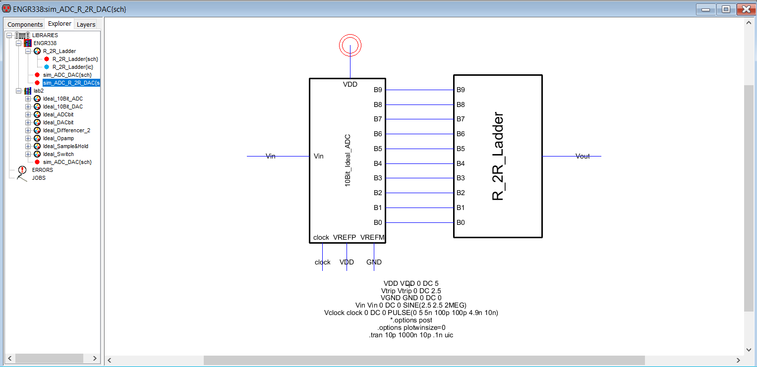
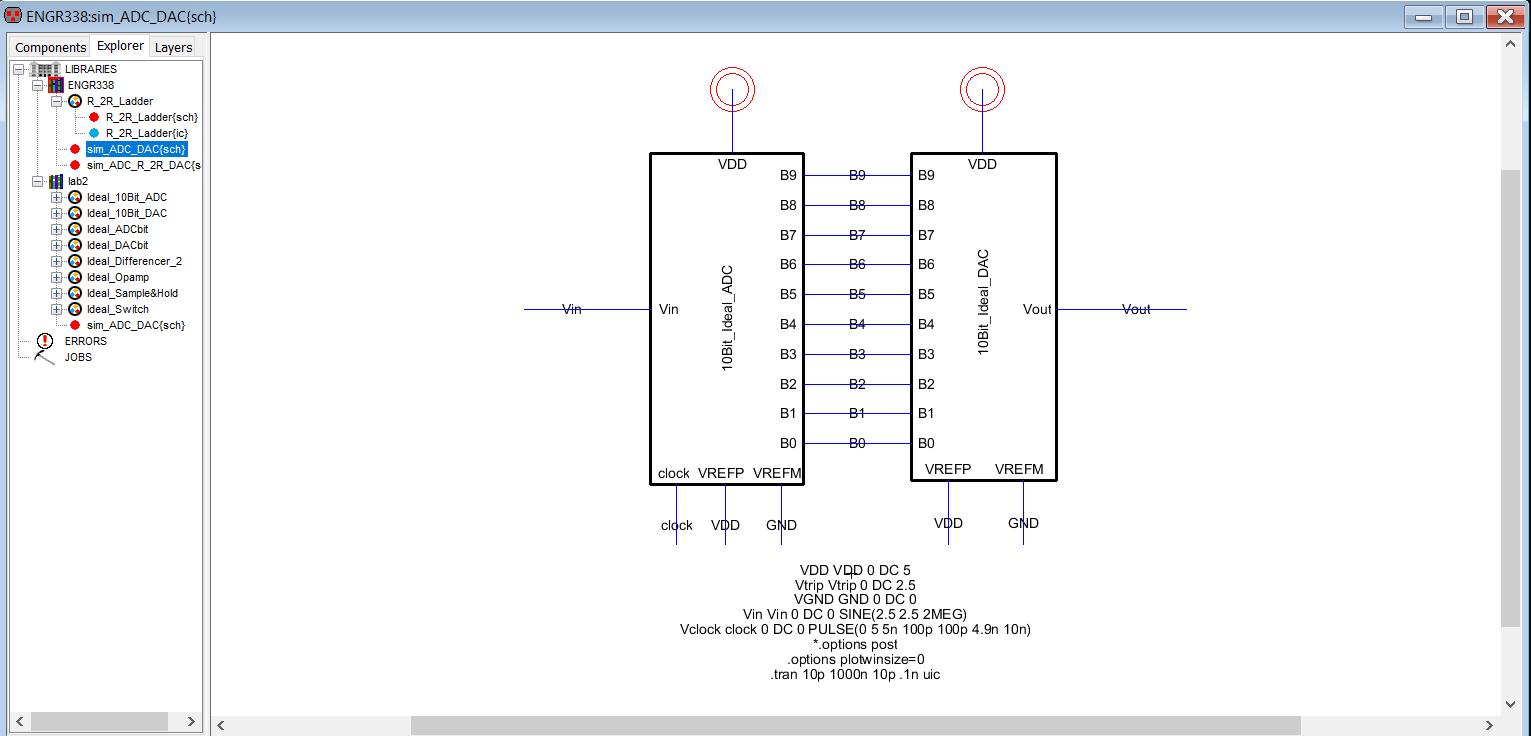
Figure 1: Schematic view of the ideal ADC/DAC.
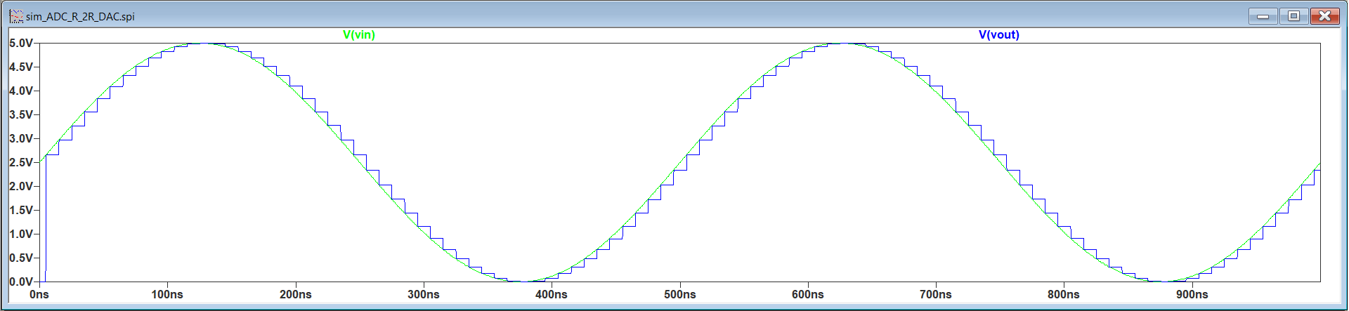
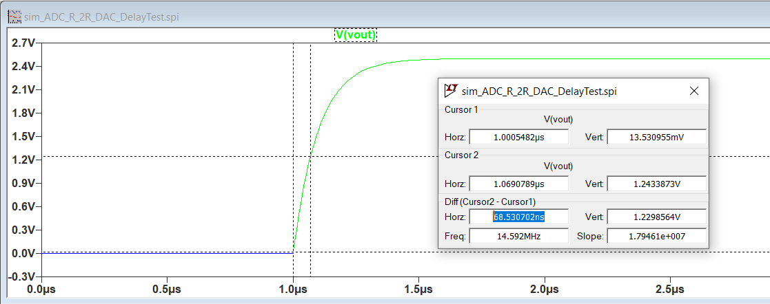
Figure 2 shows the simulation results from LTspice.


Figure 2: Simulation of ideal ADC/DAC.

Task 2: DAC Design and DAC/ADC Simulation

The R-2R DAC design is a simple resistor ladder. The n-well resistor ladder used to form the DAC is shown in Figure 3.


Figure 3: n-well resistor ladder.


The DAC design will be used in future labs, so an icon was made for the DAC (Figure 4).


Figure 4: Icon for the DAC.

The DAC was then combined with the ADC from task 1.


Figure 5: Combined DAC and ADC.

The design was then simulated in LTspice.


Figure 6: Simulation of DAC and ADC.

Task 3: Testing the Time Delay of the DAC


All input pins of the DAC were grounded, except for pin B9. A pulse function was connected to pin B9 and the output of the DAC was coupled to ground using a 10pF capacitor (Figure 7).


Figure 7: Time delay test of the DAC.


The circuit was converrted into its thevenin equivalent (Figure 8).


Figure 8: Thevenin equivalent of the DAC circuit.

A time delay of 0.7RC = 0.7 * 10k * 10pF = 70n seconds is expected at the output.
LTspice shows that the expected delay is correct (Figure 9).


Figure 9:
LTspice simulation of the circuits time delay.


Discussion:

This lab  discussed the design and simulation of a R-2R DAC using ElectricVLSI. The simple DAC was formed using an n-well resistor ladder. The DAC was combined with an ADC to test the output step size of the DAC. Simulations were performed throught the design process. The time delay of a DAC circuit was also calculated and confirmed with a simulation.