1. 8-Bit Sucsessive Approximation Register Analog to Digital Converter Designed with Electric VLSI 2. The purpose of this
lab is to build and simulate an 8-bit SAR ADC and build all componets
assocated with the SAR ADC including the Sample and Hold, Comparator,
Biasing, Circuit, Texas Instruments D-Type Flip Flop, Timing Block,
SAR, R2R ladder, Door Register, Buffer, and 3 input NAND gate.
Objectives: 1. Duplicate the work in ElectricVLSI and keep clean Library for future use. 2. Use C5 technology changing the voltage from 5 V not 1 V. 3. Include simulation results, discussions, and DRC clean of each function block. 4. Answer all relavent questions for the tutorial.
3. Materials and Methods
LTSpice computer Application
Paper and Pencil
Electric VLSI Application
4. Results
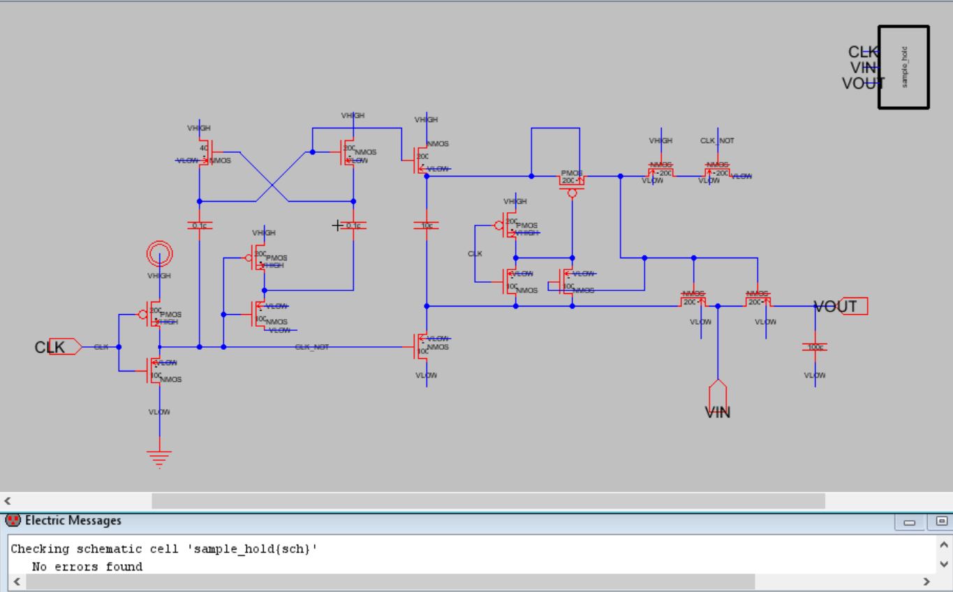
Figure 1. Schematic of sample and hold shown using C5 technolgy of Electric with clean DRC.
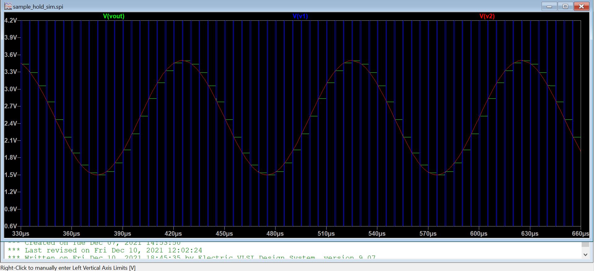
Figure 2. Simulation of the Sample and Hold shown to be tracking the analog voltage and holding voltage for the SAR.
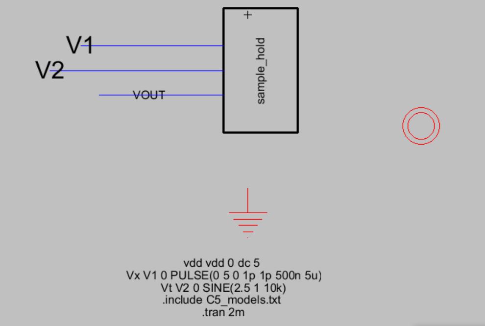
Figure 3. Simulation code and icon used for LT Spice.
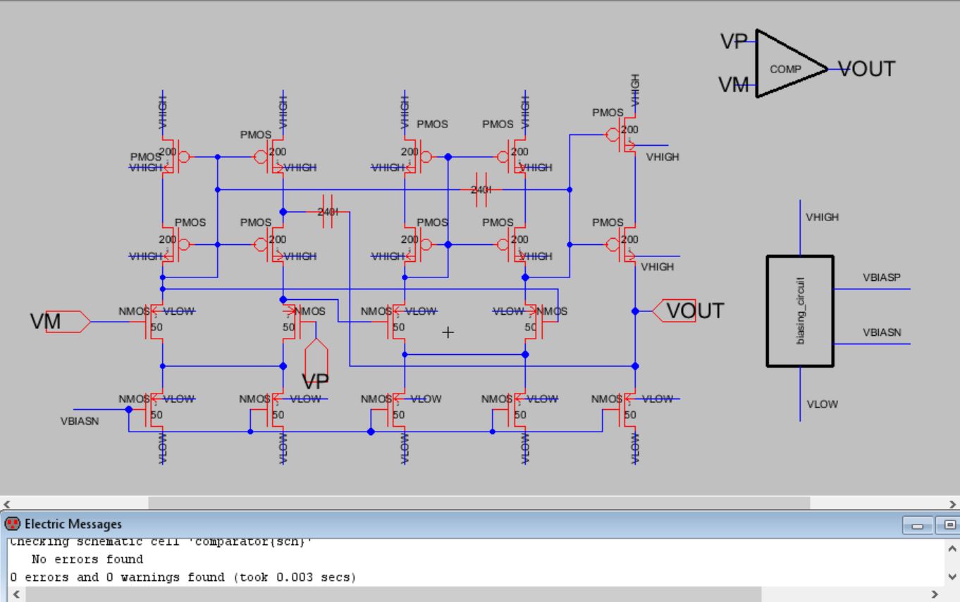
Figure 4. Operational
Amplifier or Comparator shown with CMOS topology and exported pins to
create Operational Amplifier Icon.
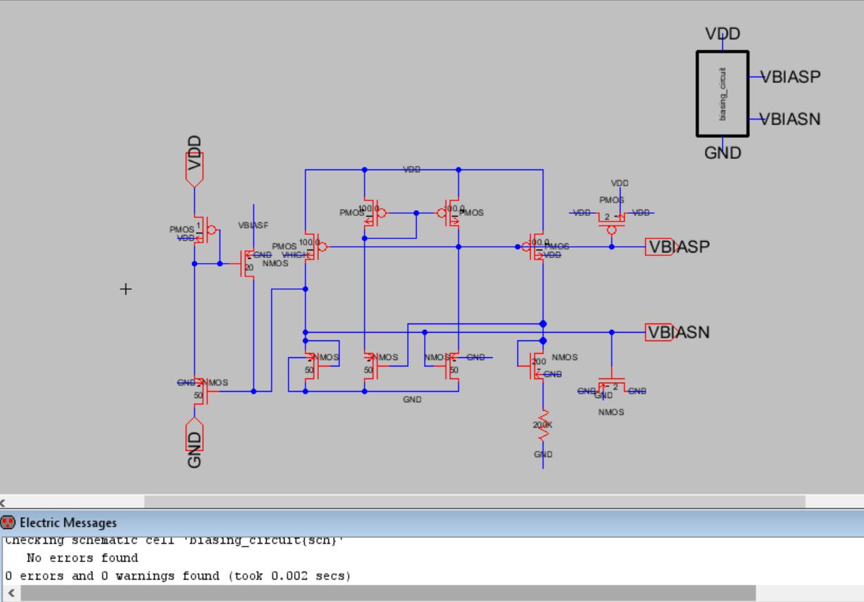
Figure 5. Biasing
Circuit used for the Operational amplifer logic used as a smaller
component in larger operational amplifer to carry out comparisons of
voltages.
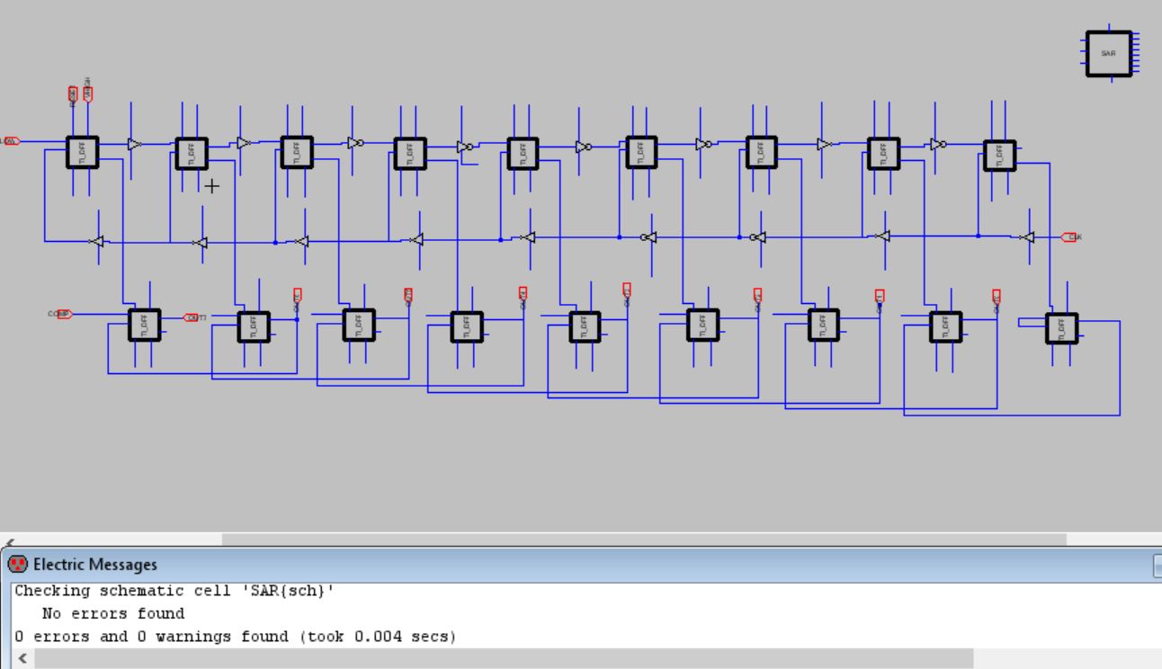
Figure 6. Sucsessive Approximation Regisiter shown with clean DRC and several D type Flip Flops from Texas Instruments.
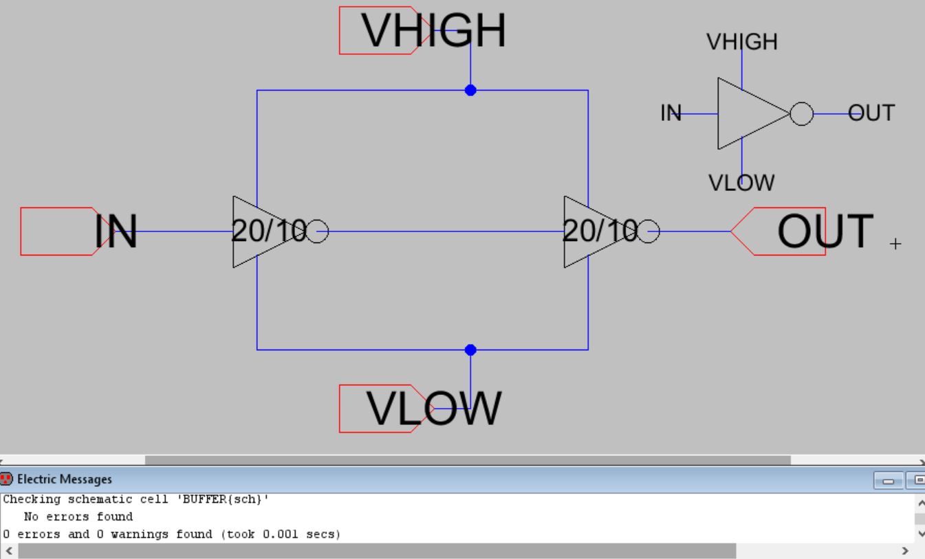
Figure 7. Buffer used to slow logic between the TI DFF's with in the SAR.
Figure 8. Simulation of SAR using icon of schematic and various voltages shown using LT spice.
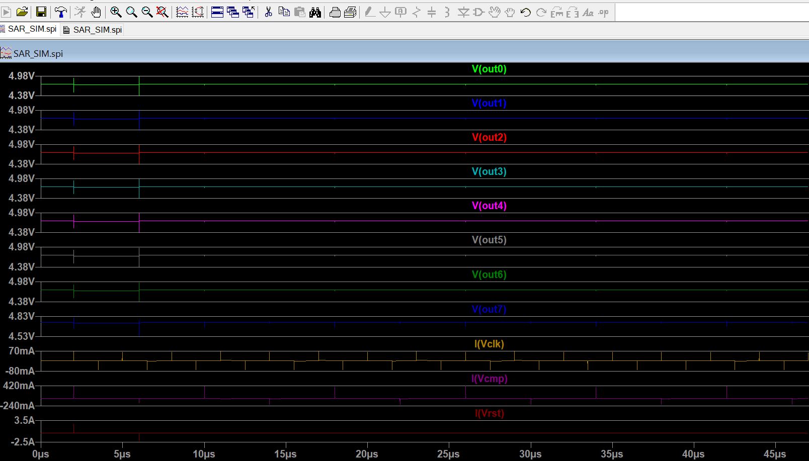
Figure 9. Simulation of the SAR logic shown using various voltages and using C5 technolgy with a 5 V power source.
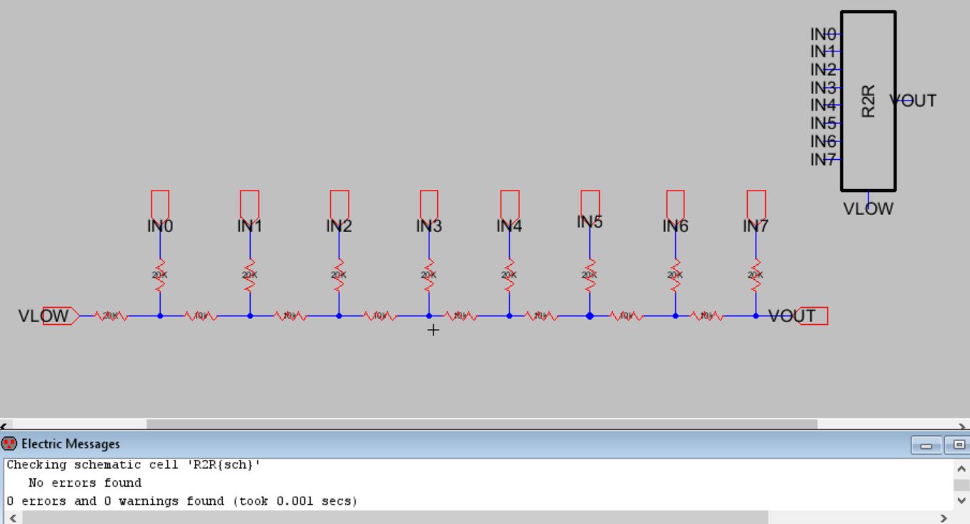
Figure 10. R-2-R ladder used for reproducing the digital voltages in the SAR ADC shown with clean DRC.
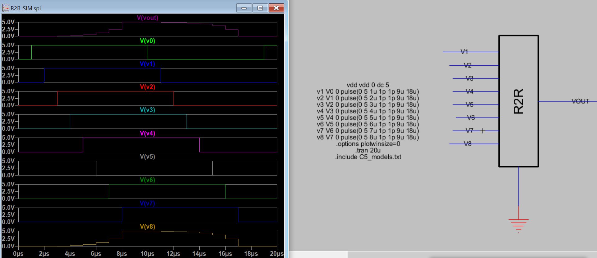
Figure 11. R-2-R ladder simulation given by several pulse functions and LT Spice simulation.
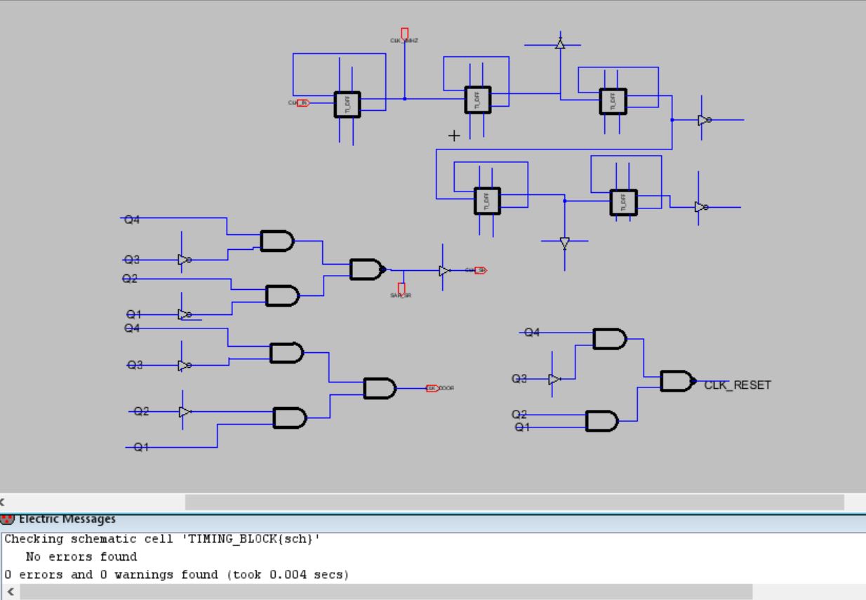
Figure 12. Timing block constructed with several NAND, AND, and inverter toplogies as well as the TI DFF shown with clean DRC.
Figure
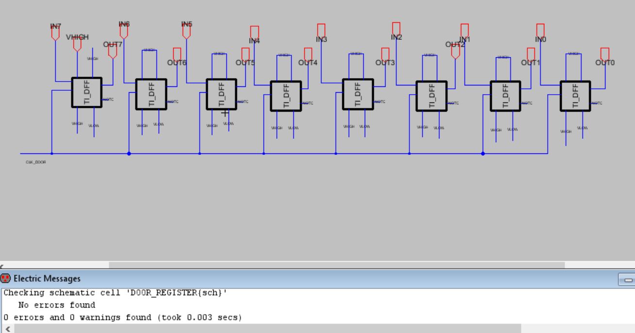
13. Door register used to release digital logic at certain times to
then be passed to one R-2-R ladder given with clean DRC.
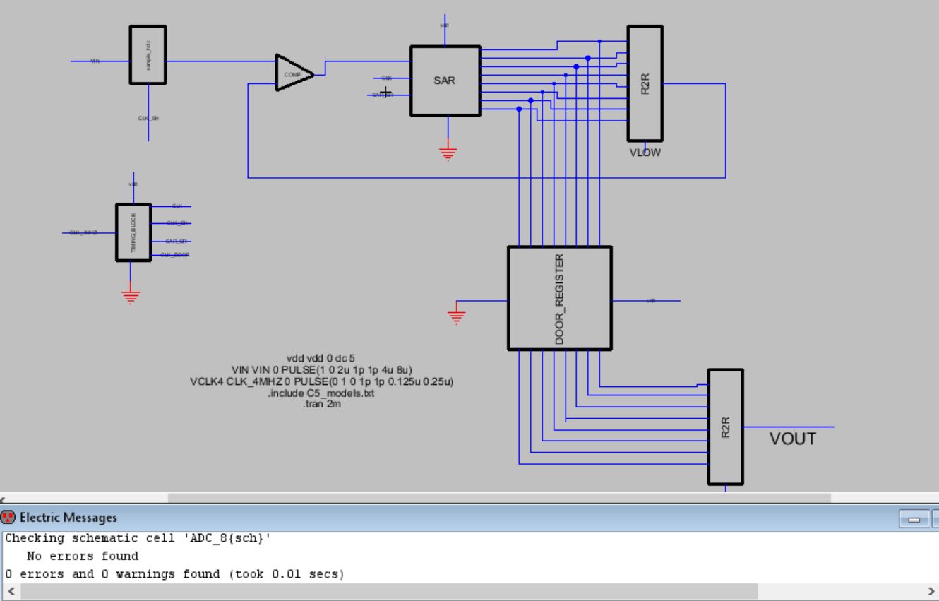
Figure 14. The final 8-Bit Sucsessive Approximation Register Analog to Digital Converter given with clean DRC.
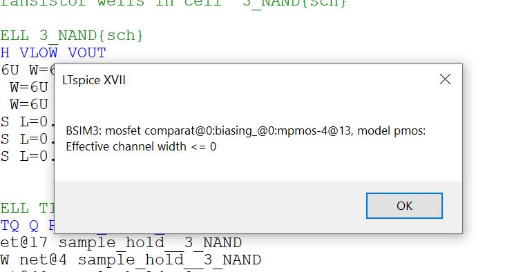
Figure 15. Error produced with no known way of solving which stopped final simulation of the 8-Bit SAR ADC.
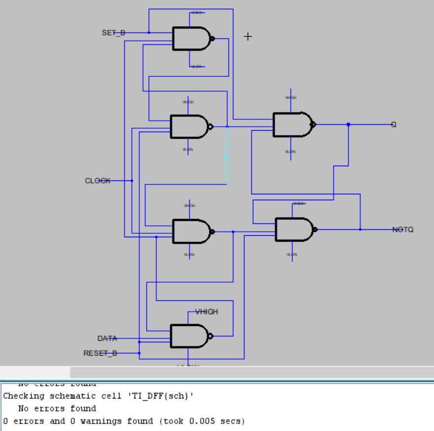
Figure 16. Texas Instruments D-type Flip Flop a key component within this SAR ADC topology shown with clean DRC.
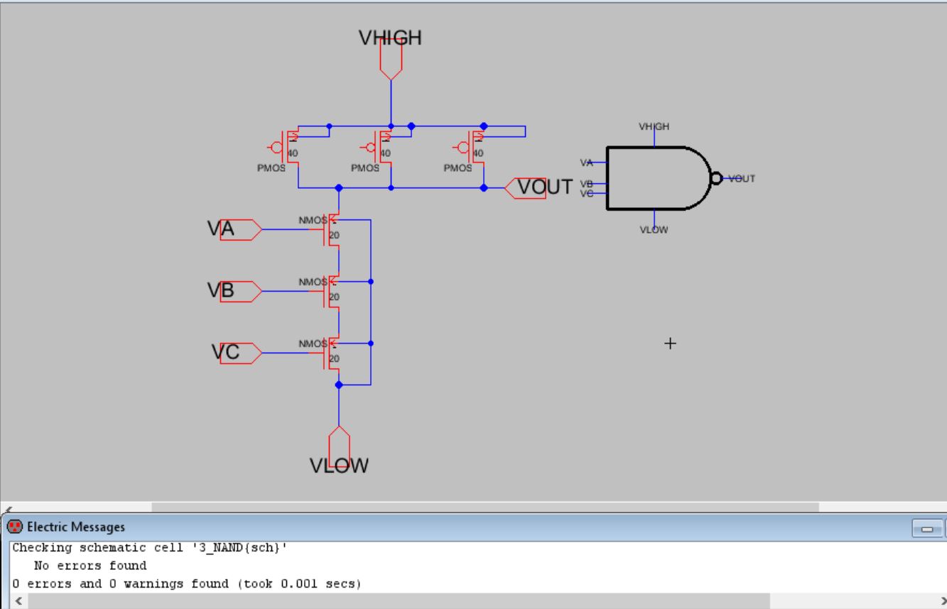
Figure 17. Underlying CMOS transistor topology of the 3 input NAND used to create the TI DFF.
5. Discussion Audra's
circuit has a timing issue looks like the clodks could be off yeilding
a delay of the sampled signals. The dip at the beginning of the
simulation is most likely the power of the circuit ramping up and once
the sufficent power is achieved the SAR can begin to track. One
shouldn't use the output of the sample and hold because its not a
digital signal these are approximated analog voltages being held.
This
lab was challenging many components in components. It was hard to
simulate the blocks as more review is needed on how to correctly carry
out spice code. The schematics were not as hard to build but took a
great deal of time to create. The greatest challenge was the LT spice
code and will need further improvment for future labs. Overall the
project helped to obeserve all components of the SAR ADC and reinforce
Digital electronic material.