1. Layout the R-2R DAC 2. The purpose of this lab was to build a layout of the R-2R DAC
(version 2), pair the R-2R DAC with an ideal ADC, and finally to run a
simulation of this creation. To simulate Electric VLSI was used,
then LTSpice to give a visual representation.
3. Materials and Methods
LTSpice computer Application
Paper and Pencil
Electric VLSI Application
4. Results
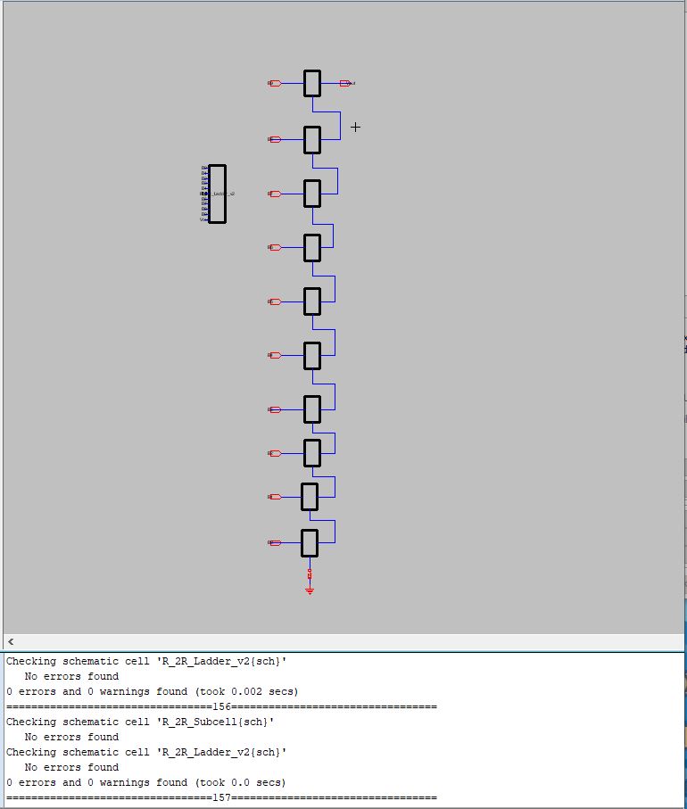
Figure 1. Schematic of subcells for the R_2R_Ladder created using electric VLSI, shown with clean DRC.
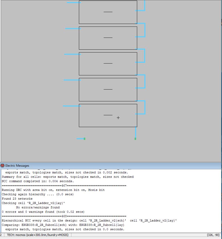
Figure
2. R-2R Subcell Layout created using Electric VLSI. Design created
using three N-well resistors stacked on top of another and wired
together. Then 10 of these were wired together and exported with names
B9-B0. Subcell Layout shown with clean DRC and NCC.
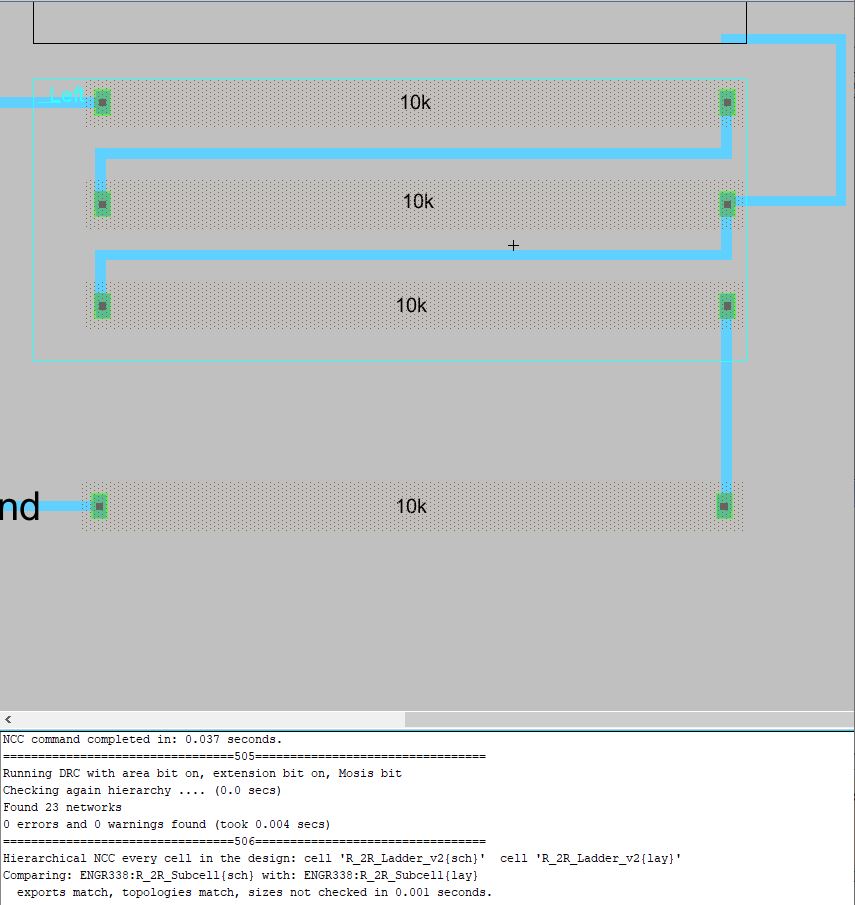
Figure 3. R-2R DAC shown using N-Well resistors in Layout view.
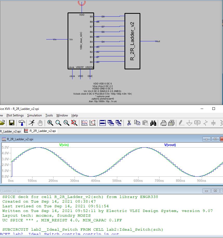
Figure 4. R-2R DAC and ideal
ADC paired and simulated using LTspice showing the voltage pulse in and
the replicated digital data out.
5. Discussion
Electric is an effective tool for the layout of the R- 2R DAC and
ADC. The LTSpice simulations helped to verify that analog voltage data
is being converted to digital data. The lab helped to produce layout
schematics of the R_2R ladder and create more consise forms of the
logic shown.