1. More about Seven Segment Display and Others
2. The purpose of this lab was to learn more about programming within
vivado and uploading that code to the FPGA device. Several gates were
created including the inverter, 2-bit full adder, 8 bit AND, and 4-1
MUX gates. These gates were simulated and testing using leds and
switches on the FPGA device. Then we accessed the 7 segment display to
dispay numbers using binary switches and create a running led.
3. Materials and Methods
FPGA Device
Paper and Pencil
Vivado Application
4. Results
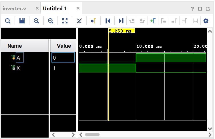
Figure 1. Simulation of inverter shown using a test bench in
Verilog.
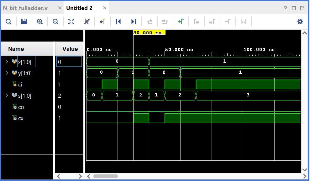
Figure
2. Simulation of the logic of the 2-bit full adder shown
using a test bench created in Verilog.
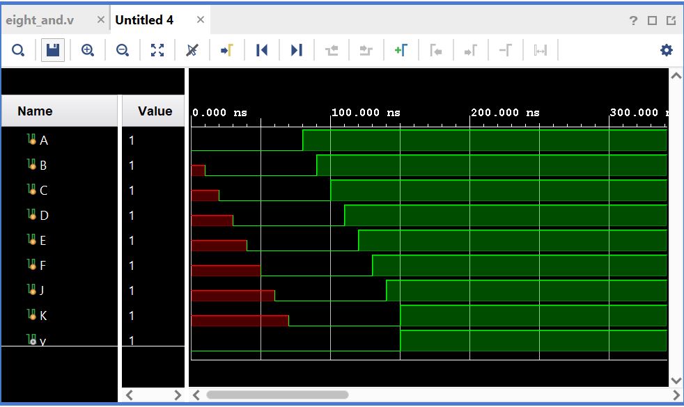
Figure
3. 8 bit AND gate simulation shown using a test bench created
using verilog.
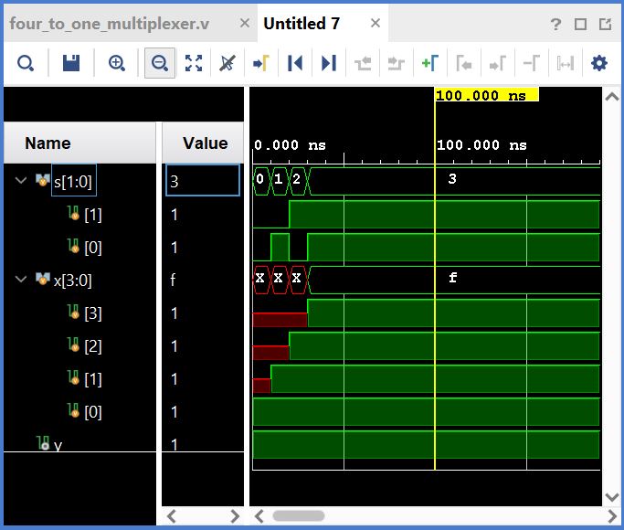
Figure
4. Logic of the 4-1 multiplexer created using a test bench
using verilog.
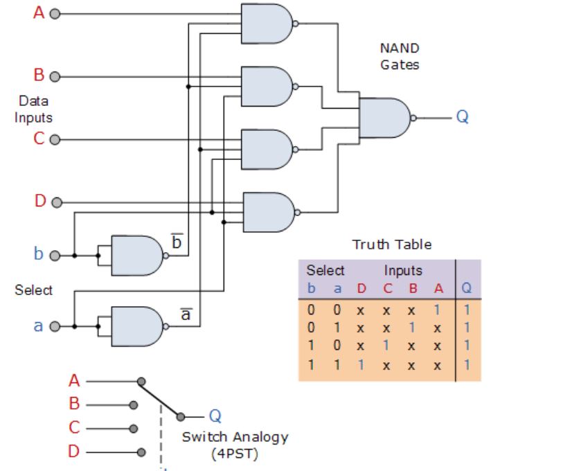
Figure
5. Truth table of 4-1 mux logic and schematic.
(electronic.tutorials.ws)
Figure
6. Demonstration of the inverter, 2- bit full adder, 8 bit AND, and 4-1
mux logic gates using leds and switches.
Figure 7. Demonstration of the Running Leds, seven segment display (4SSDs), and singular SSD. (missing code included 4'b0000 statement allowing certain SSDs to be turned on) 5.
Discussion
The Verilog code is challenging and not something I have seen
before it takes a certain amount of trial and error and experimenting.
The code is simple and effective and there is still much to learn of
the facuets of the Verilog language. Overall the vivado application and
FPGA device are a very effective tool once the code becomes clear.
Instead of all logic gates being wired by hand and coded by Arduino
they are exacuted all in the Vivado application.