1. Introduction to FPGA
2. The purpose of this lab was to learn the basics of Viviado as it
applies to uploading and designing logic gates including XOR, AND, and
OR gates. These were designed using the verilog code, tested on a test
bench, and then tested by using the LED's on the FPGA device.
3. Materials and Methods
FPGA Device
Paper and Pencil
Vivado Application
4. Results
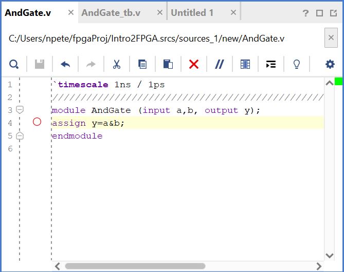
Figure 1. Verilog code used to create AND gate in Vivado.
(Similar logic used for OR and XOR with subsitution of "&" with
"|" and "^")
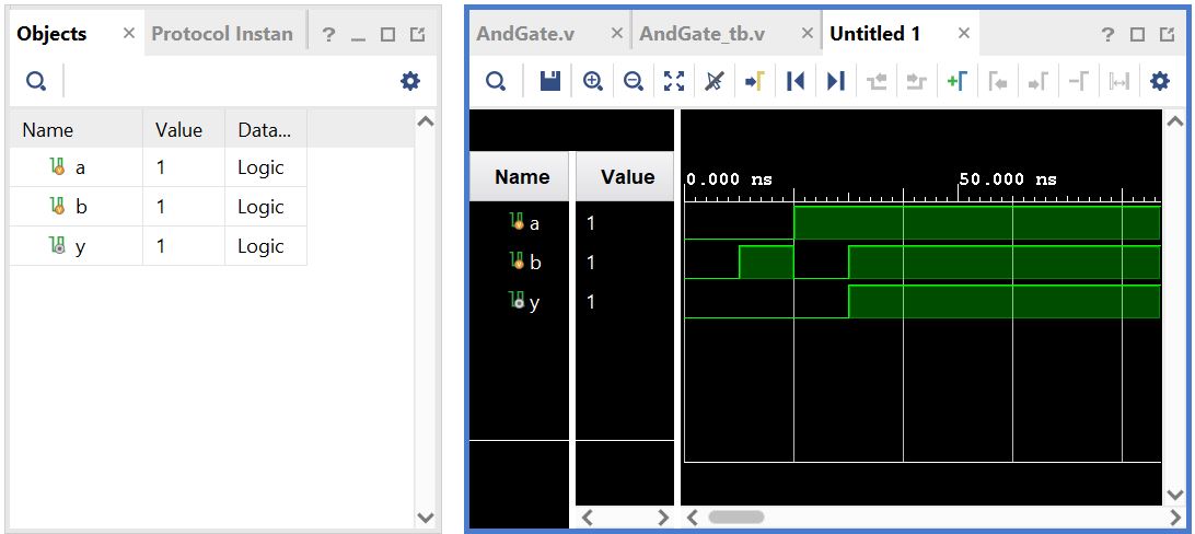
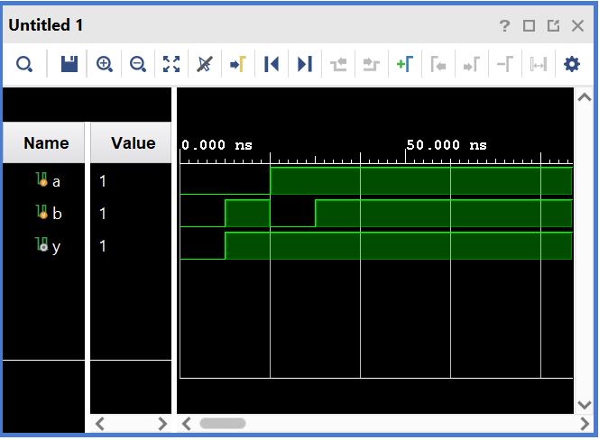
Figure
2. Logic of AND gate shown using test bench in Vivado.
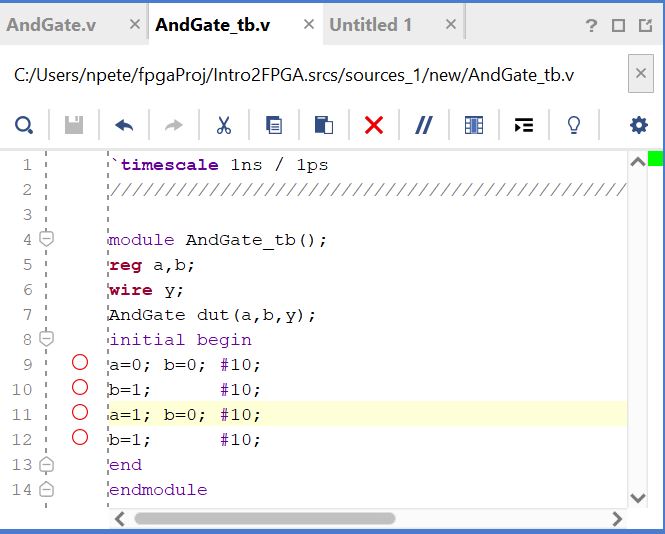
Figure
3. Verilog code used to create AND, OR, and XOR gate test
bench and simulate AND, OR, and XOR logic with minor modifications
between each.
Figure
4. Logic of OR gate shown and simulated with a simular
testbench used for AND gate.
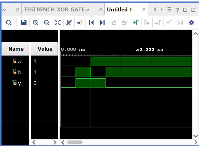
Figure
5. XOR gate simulated using simular test bench as AND gate.
Figure
6. OR gate simulation using volatile methods and led's to
simulate output.
Figure 7. OR
gate simulation using non-volatile methods and led's to simulate output.
Figure
8. XOR
gate simulation using volatile methods and led's to simulate
output.
Figure
9. XOR
gate simulation using non-volatile methods and led's to simulate
output.
5.
Discussion
The Vivado interface is a tool that is navigated well and there is
not to much resistance once one knows the flow of implementing logic
gates. The actual simulation of the logic gates using led's and
Vivado is powerful and allows the users to fully access and build logic
in FPGA's.