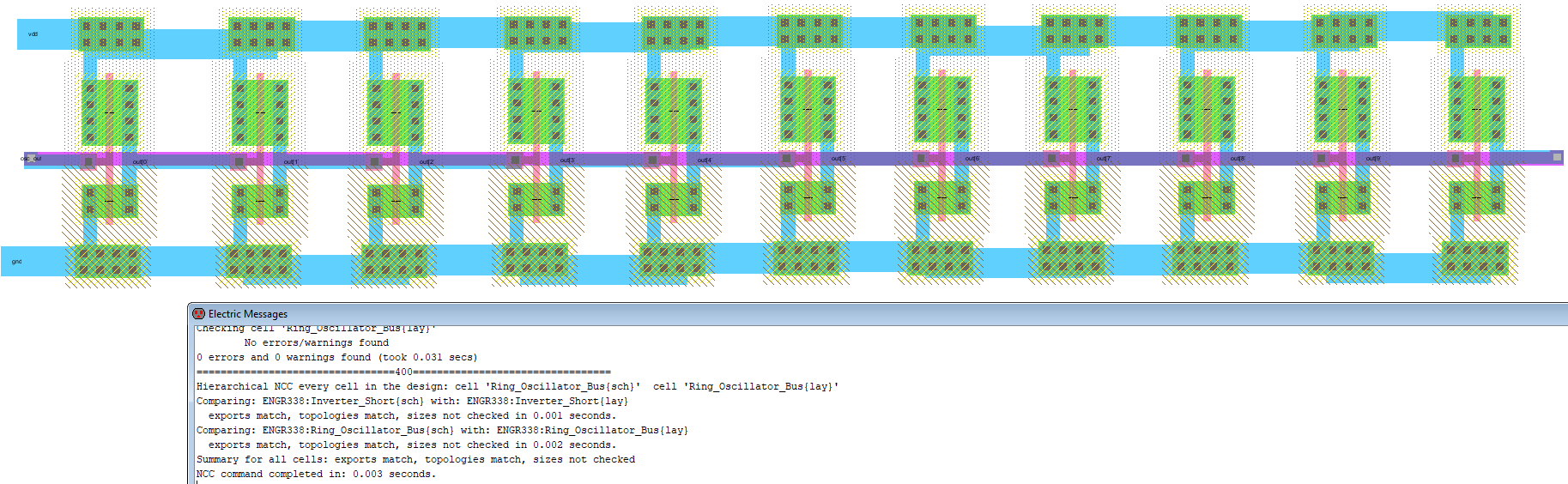
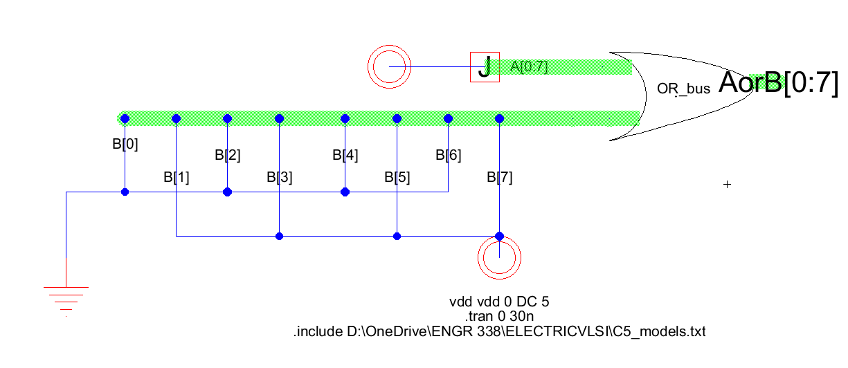
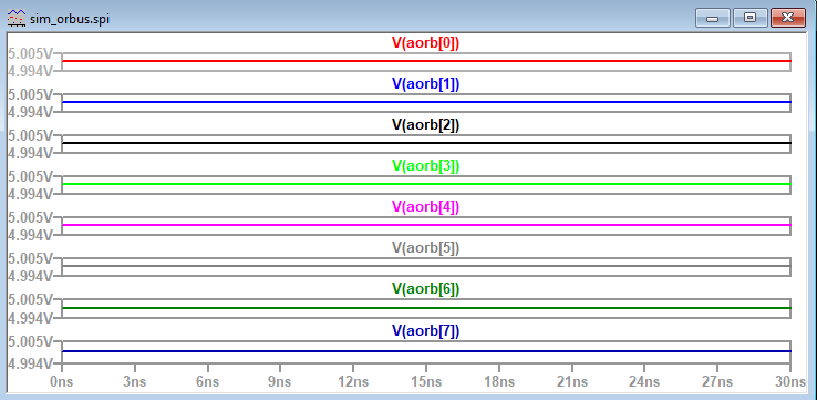
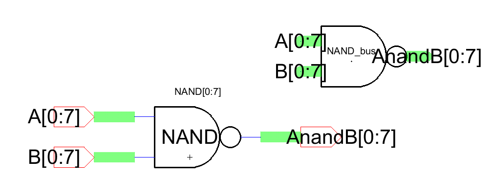
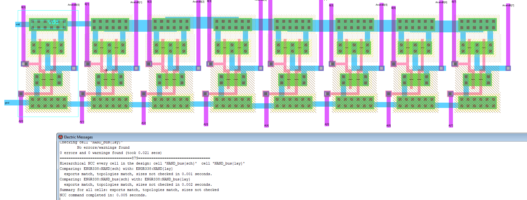
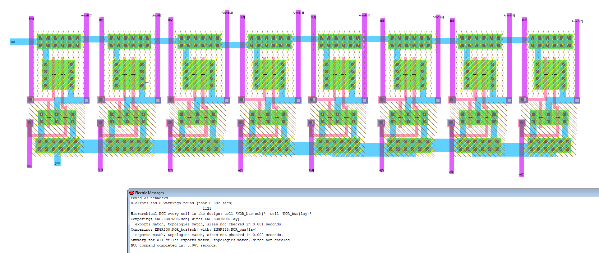
ENGR338 Lab 2021 Spring
Lab 7
Name:
Nicolas Llarena
Email: Njllarenaarias@fortlewis.edu

1. Lab 7 -
Using Buses in Electric VLSI
2. Introduction
The Purpose of this lab is to get more familiar with Electric VLSI by creating 8-bit NAND, NOR AND, and OR gates. We will also build a ring oscillator using buses. All of these gates will be simulated in LTSpice to check that everything works correctly. The layouts will have to be built carefully since they might be time consuming and large.
3. Materials
Materials Quantity
LTSpice Software
1
Calculator
1
ElectricVLSI Software
1

4. Results

Task 1


       Figure 1.  Building the schematic for the Ring oscillator the first way.
         
         
Figure 2. This Figure shows the simulation of the first ring oscillator.

      
Figure 3. The schematic for the second ring oscillator using busses is shown above as well as error checks and a simulation on LTSpice.


Figure 4. This Figure shows the complete layout of the Ring oscillator.

Task 2


Figure 5. A schematic for the nand gate was built using the nand gate and adding an inverter.


Figure 6. After creating the schematic for the AND gate, an 8-bit AND gate schematic was made using busses.

      
Figure 7. After creating the schematic for the 8-bit AND gate, a simulation was ran to check that it is working as intended.


Task 3


Figure 8. Figure above shows the schematic and the simulation for the OR gate made in Electric VLSI.


Figure 9. Figure above shows the layout for the OR gate.


Figure 10. Figure above shows the complete layout for the 8-bit OR gate.

      
Figure 11. After creating the schematic for the 8-bit OR gate, a simulation was ran to check that it is working as intended.
Task 4
      
Figure 12. The schematic and icon view for the 8-bit NAND gate.


Figure 13. After creating the schematic for the 8-bit NAND gate, the full layout was made and checked for DRC and NCC errors. everything worked correctly.

      
Figure 14. After creating the schematic for the 8-bit NAND gate, a simulation was ran to check that it is working as intended.


Task 5     


Figure 15. This Figure shows the schematic for the 8-bit NOR gate.


Figure 16. After creating the schematic for the 8-bit NOR gate, the full layout was made and checked for DRC and NCC errors. everything worked correctly.

      
Figure 17. After creating the schematic for the 8-bit NOR gate, a simulation was ran to check that it is working as intended.


Discussion
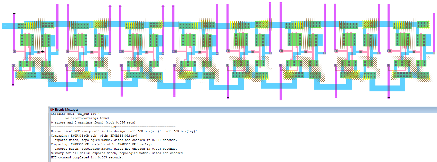
This lab was longer than I 
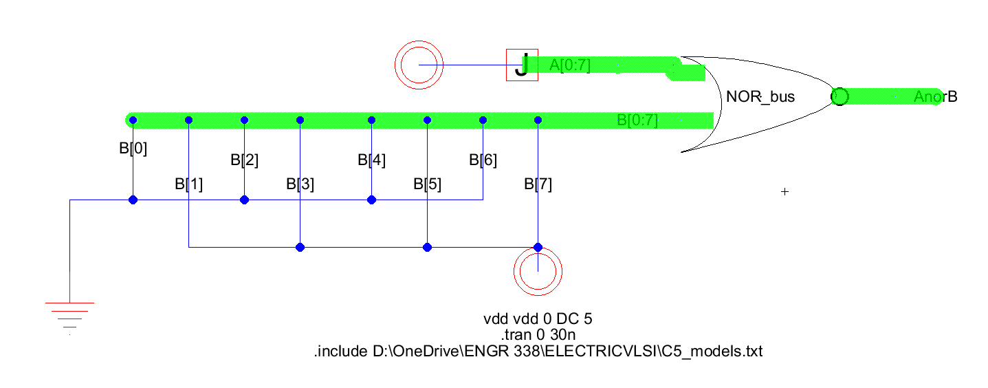
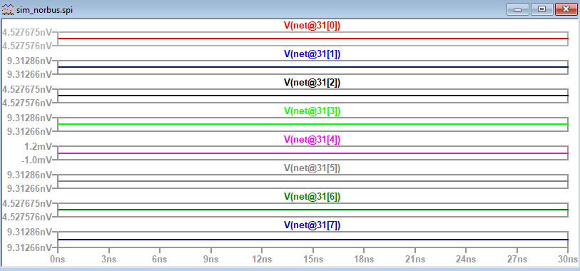
expected. The layouts for the 8-bit gates took a little bit more than usual. I was also having issues with Electric VLSI again. I was having different bugs where the program would not let me create ion views when I was having no errors. I was also having issues with the layout when everything was working correctly as far as errors went. Overall besides the issues and bugs, it was a good lab to practice with big layouts and schematics. looking forward to the last two labs.