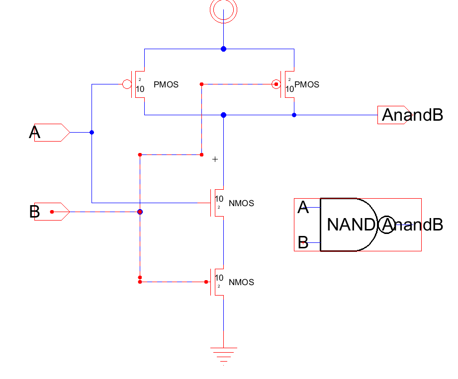
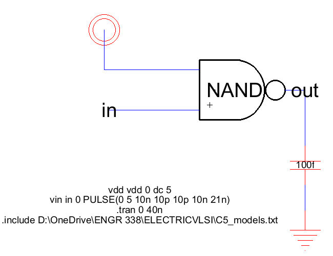
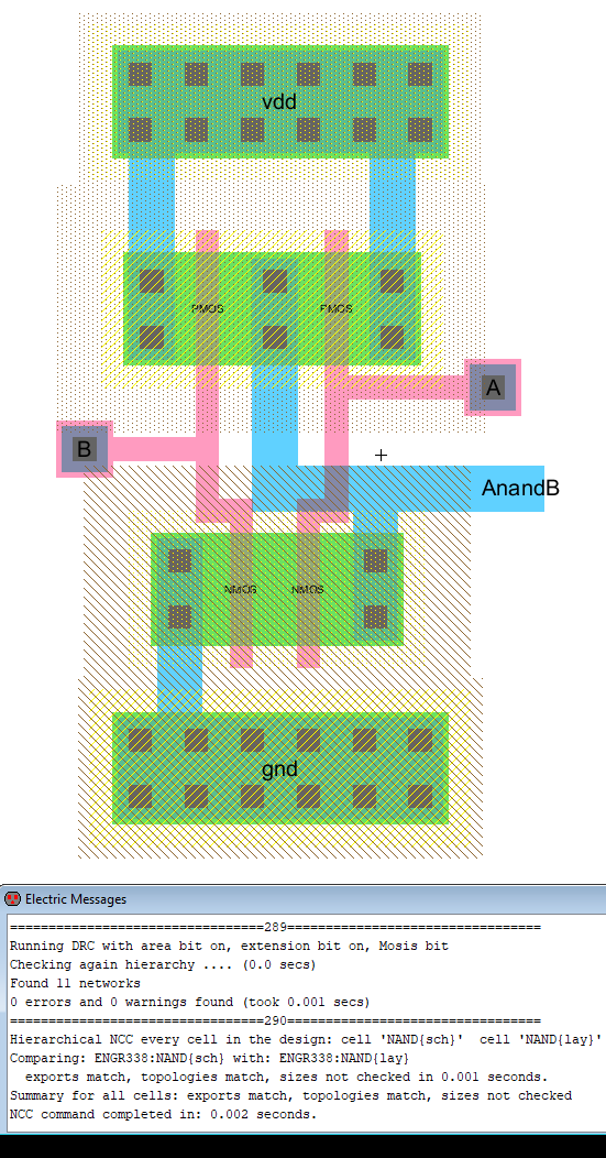
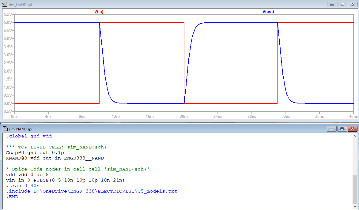
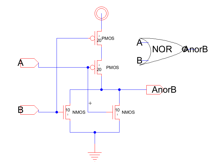
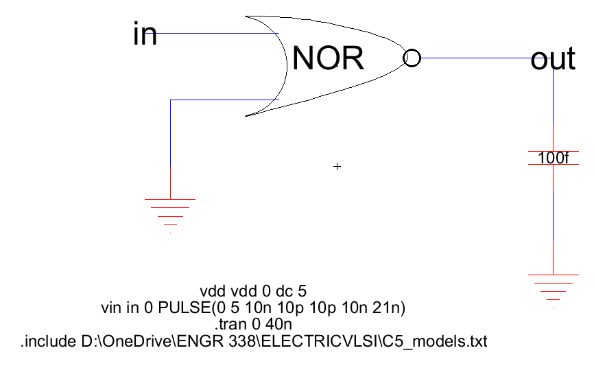
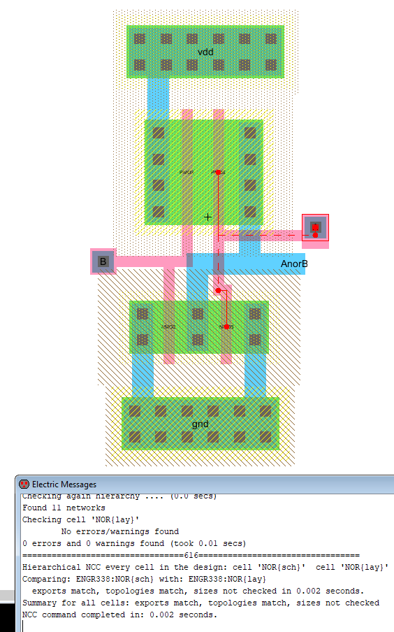
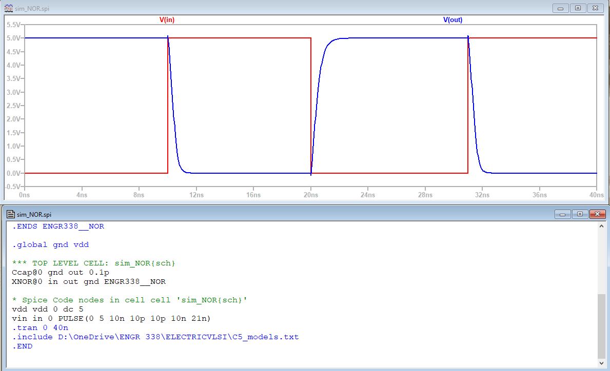
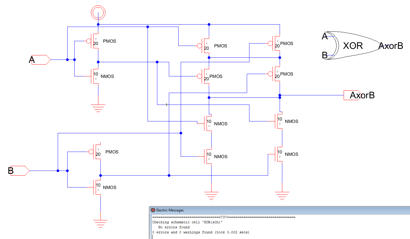
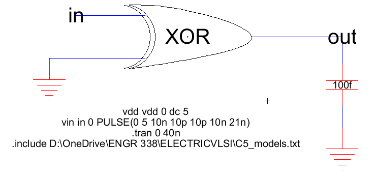
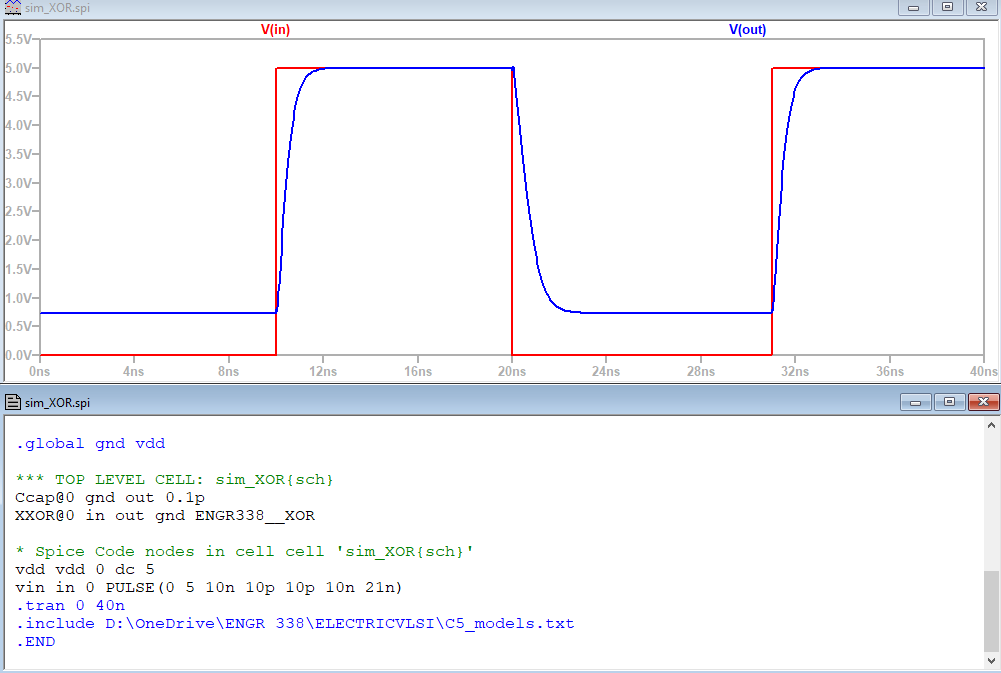
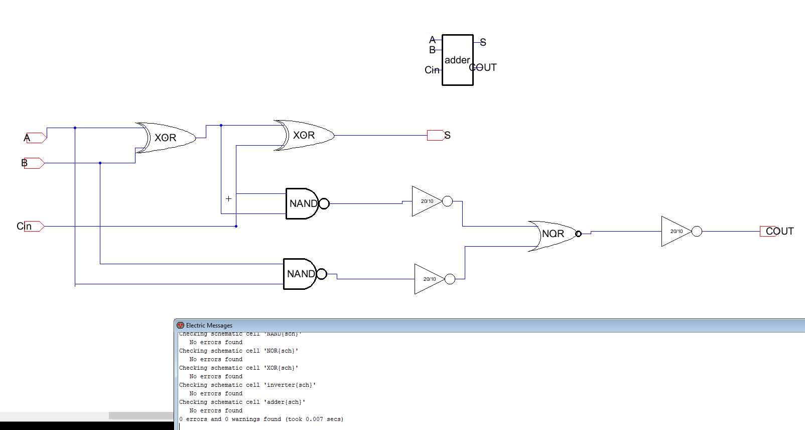
ENGR338 Lab 2021 Spring
Lab 6
Name:
Nicolas Llarena
Email: Njllarenaarias@fortlewis.edu

1. Lab 6 -
Build a NAND, NOR, XOR, and Full Adder
2. Introduction
The Purpose of this lab is to get more familiar with Electric VLSI by creating NAND, NOR, XOR, and a Full Adder. some of these layouts will take a long time to complete. Schematics, icons, layouts, and simulations will be created to learn how to do everything from start to finish. Hopefully everything goes smoothly and no errors are to be found. should be a challenging and time consuming lab.
3. Materials
Materials Quantity
LTSpice Software
1
Calculator
1
ElectricVLSI Software
1

4. Results

Task 1


       Figure 1. Creating the schematic and the simulation schematic of the NAND gate to simulate it on LTSpice.


Figure 2. After creating the schematic for the NAND gate, the layout was completed in Electric VLSI showing no  DRC errors or NCC errors. A simulation was ran on LTSpice to confirm it works as intended.


Task 2


Figure 3. Figure above shows the schematic and the simulation schematic for the NOR gate to use with LTSpice for a simulation.


Figure 4. After creating the schematic for the NOR gate, the layout was completed in Electric VLSI showing no DRC errors or NCC errors. A simulation was ran on LTSpice to confirm it works as intended.


Task 3


Figure 5. Figure above shows the schematic and the simulation schematic for the XOR gate to use with LTSpice for a simulation.


Figure 6. Figure above shows the simulation in LTSpice of the XOR gate, the layout was not completed due to running out of time.


Task 4
      
Figure 7. The schematic for the full adder was created by using the past NOR, NAND, and XOR gates we have previously made in Electric VLSI.


Figure 7. After creating the simulation schematic of the full adder, a simulation was run on LTYSpice to verify the outsputs depending on the inputs of the shcematic.


Discussion
This lab was longer than I expected. Sadly I was unable to finish some of the layouts since they are very time consuming and I had unexpected sick days that prevented me from focusing on this lab. In any case, I understand that I should have worked on this lab earlier since we had two weeks to complete it. Besides these unfortunate events, I believe the lab was a good learning experience and I learned and practiced new things in VLSI. I am now getting more comfortable with schematics and layouts. as well as custom icons for some gates. Being able to simulate schematics on LTSpice also makes this process easier and less pai