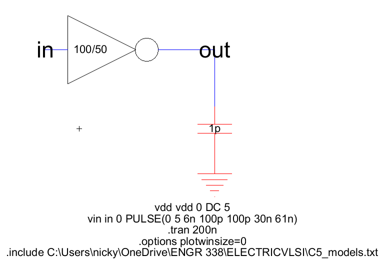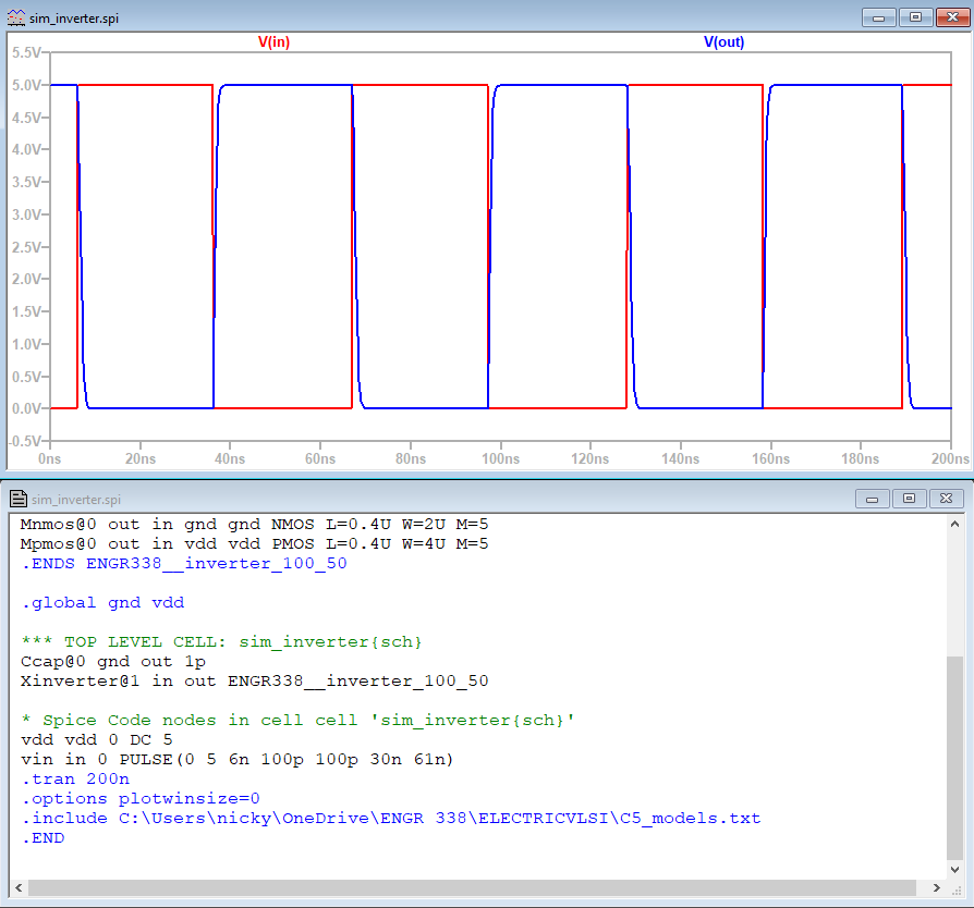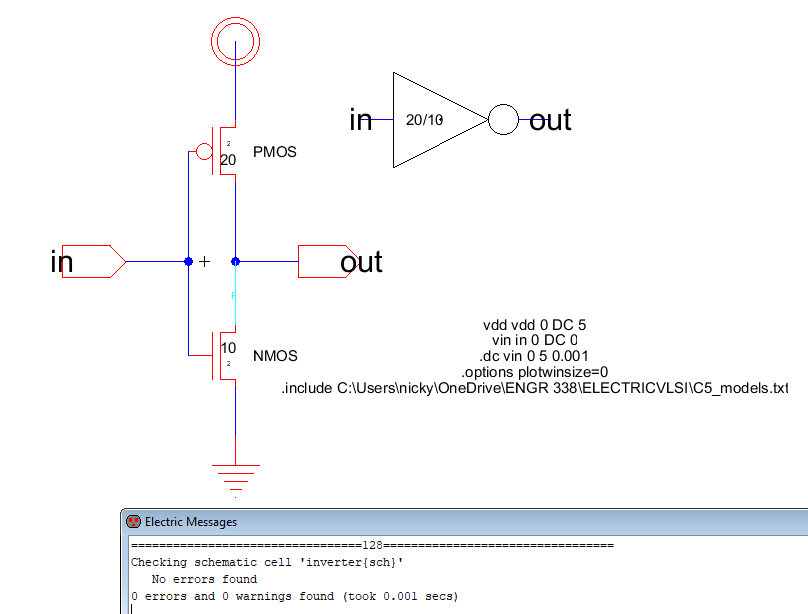
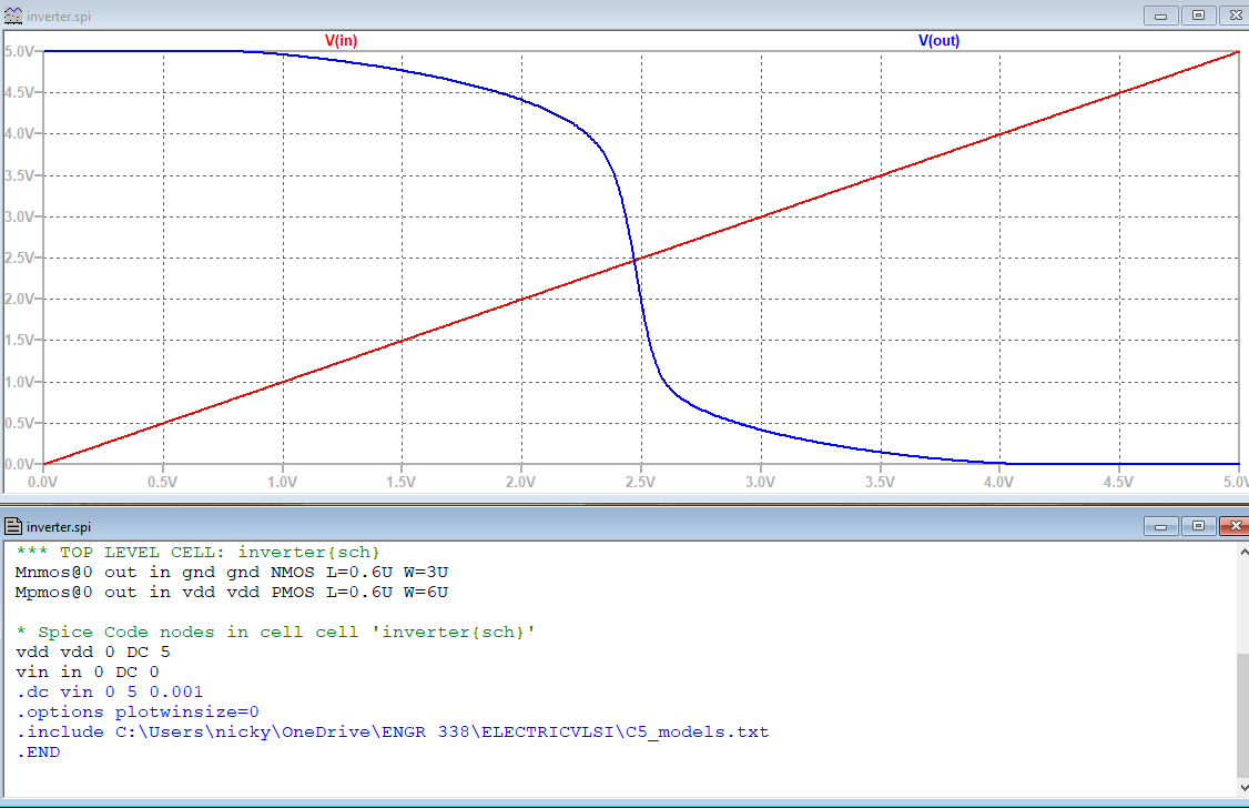
Figure 1. Creating the schematic of the first inverter. Second figure shows simulation to confirm everything is working properly.
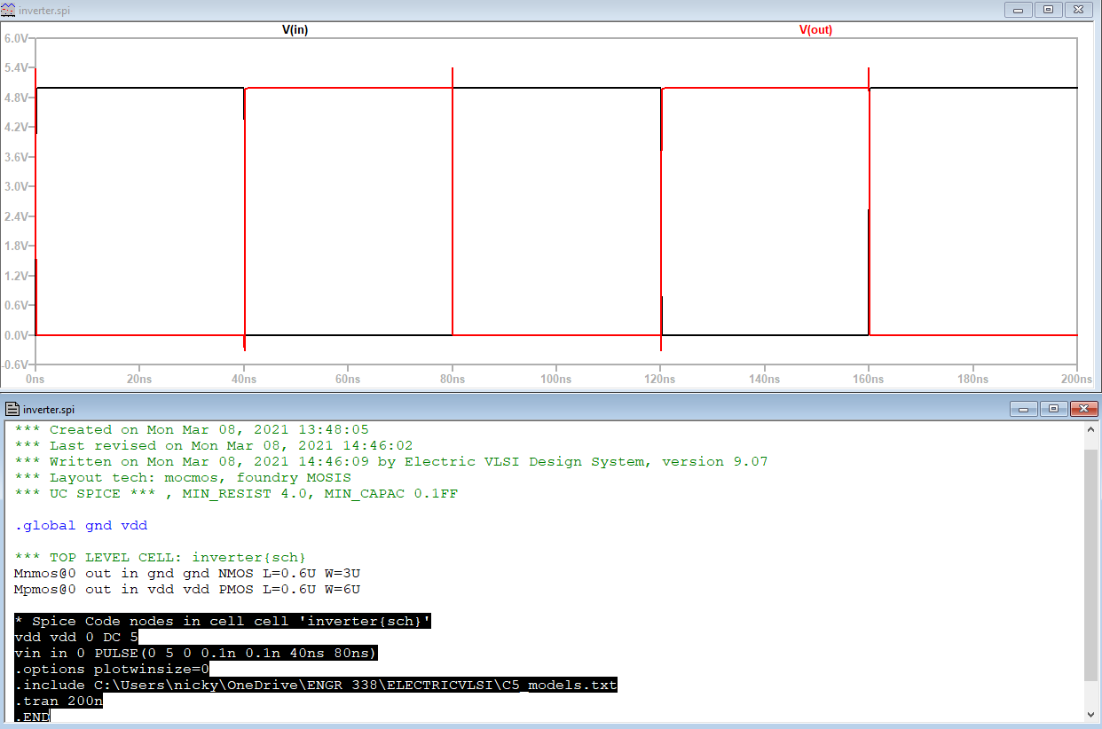
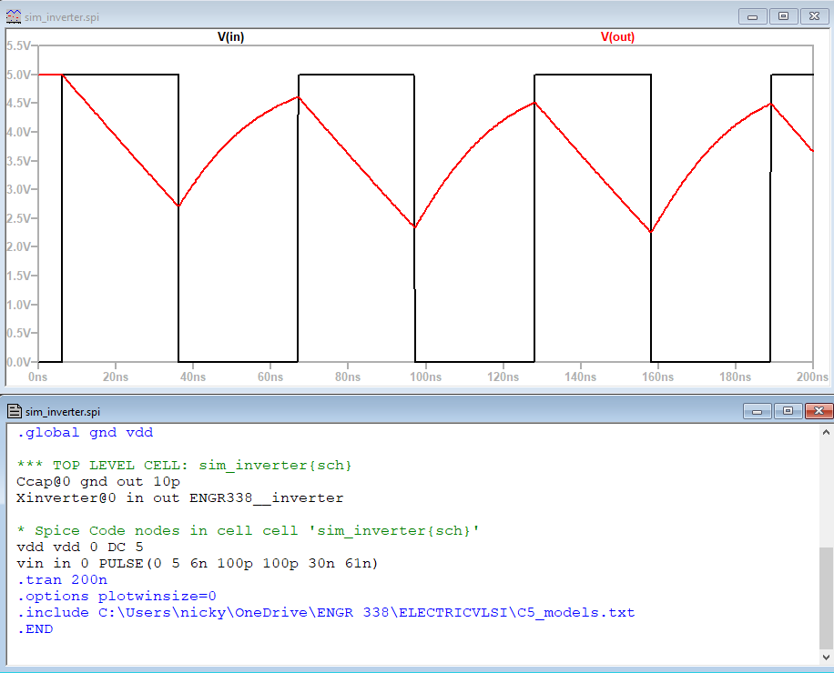
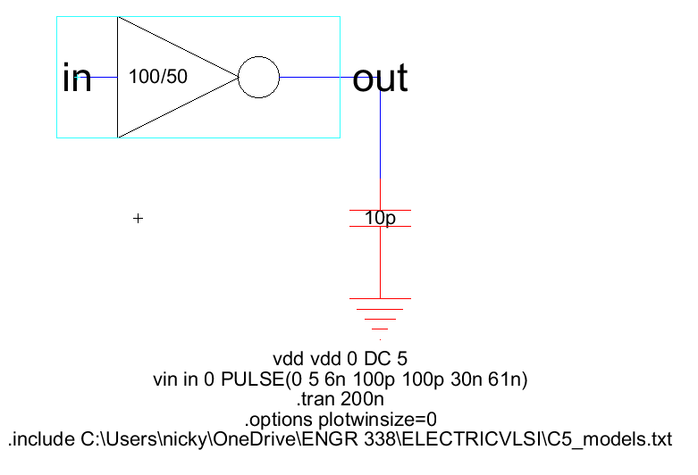
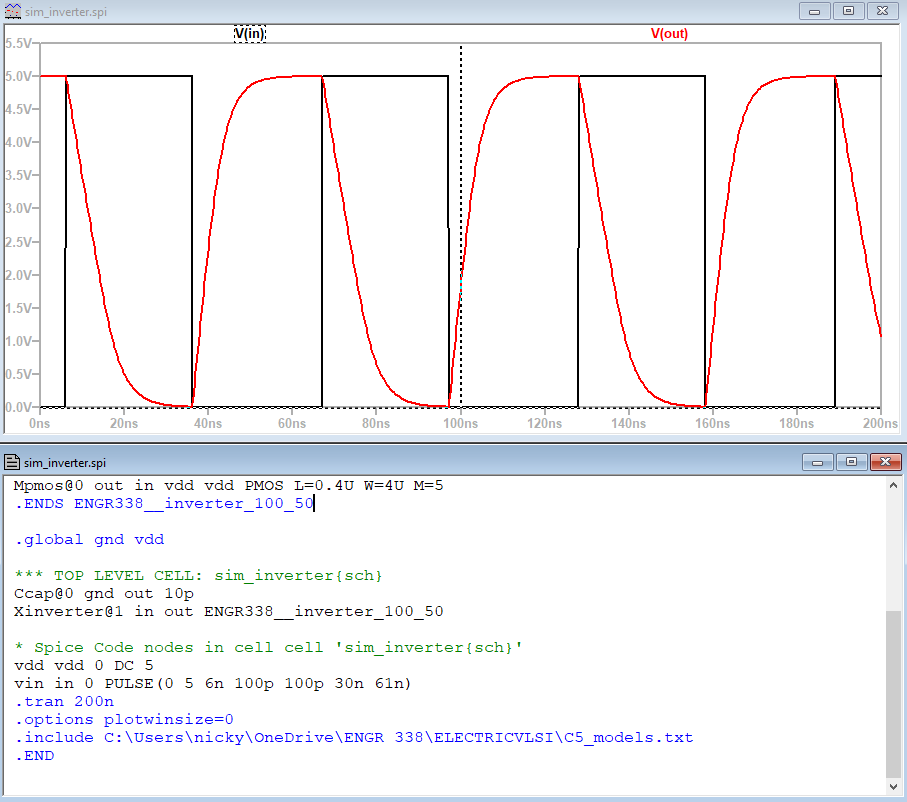
Figure 2. After confirming the inverter was working correctly, another simulation was created in LTSpice with a PULSE function.
Task 2
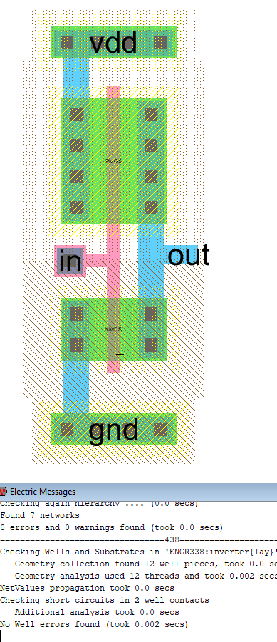
Task 3
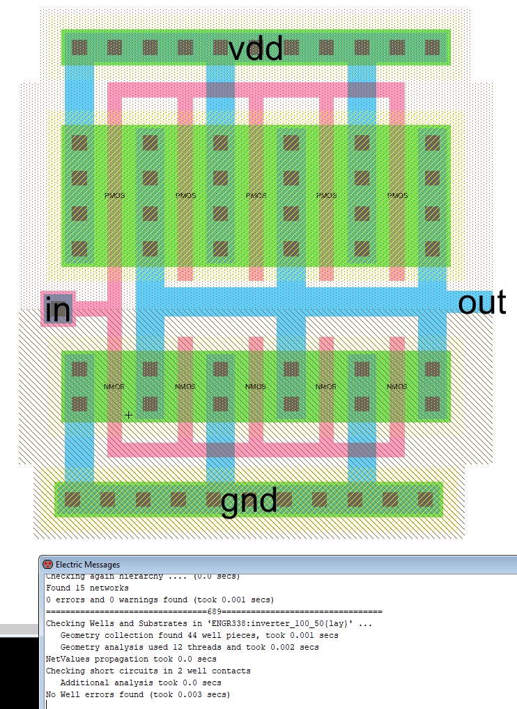
Figure 4. The
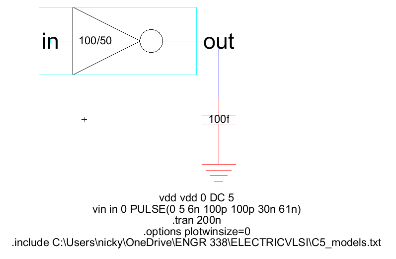
multiplier was used to build a larger inverter, the inverter layout
from task 2 was duplicated and then modified for a 100/50 inverter. DRC
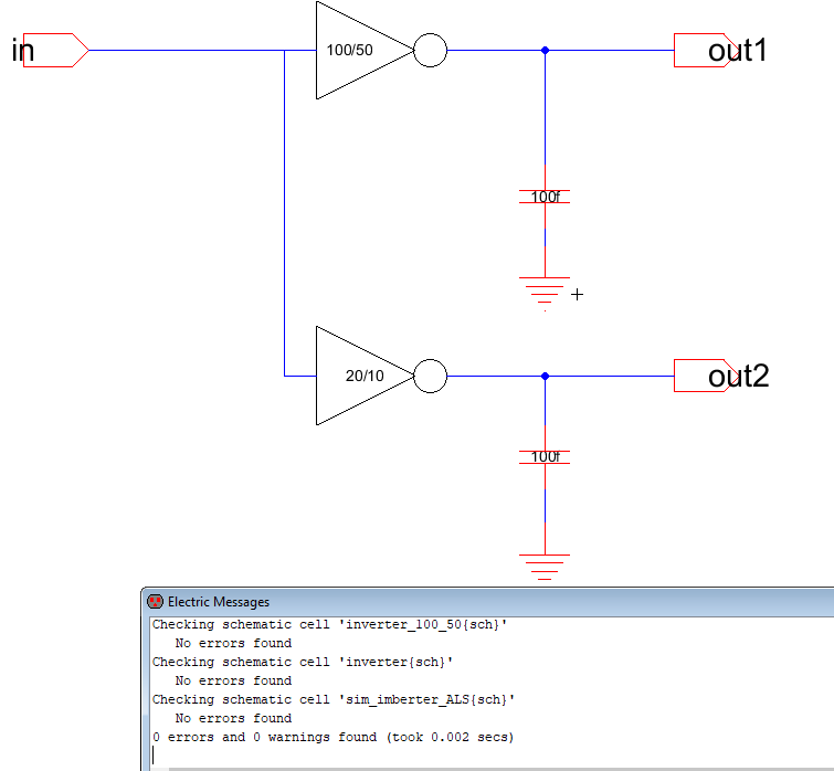
and ERC checks were made to confirm everything was working correctly.Task 4
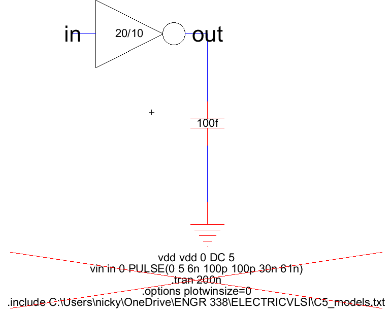
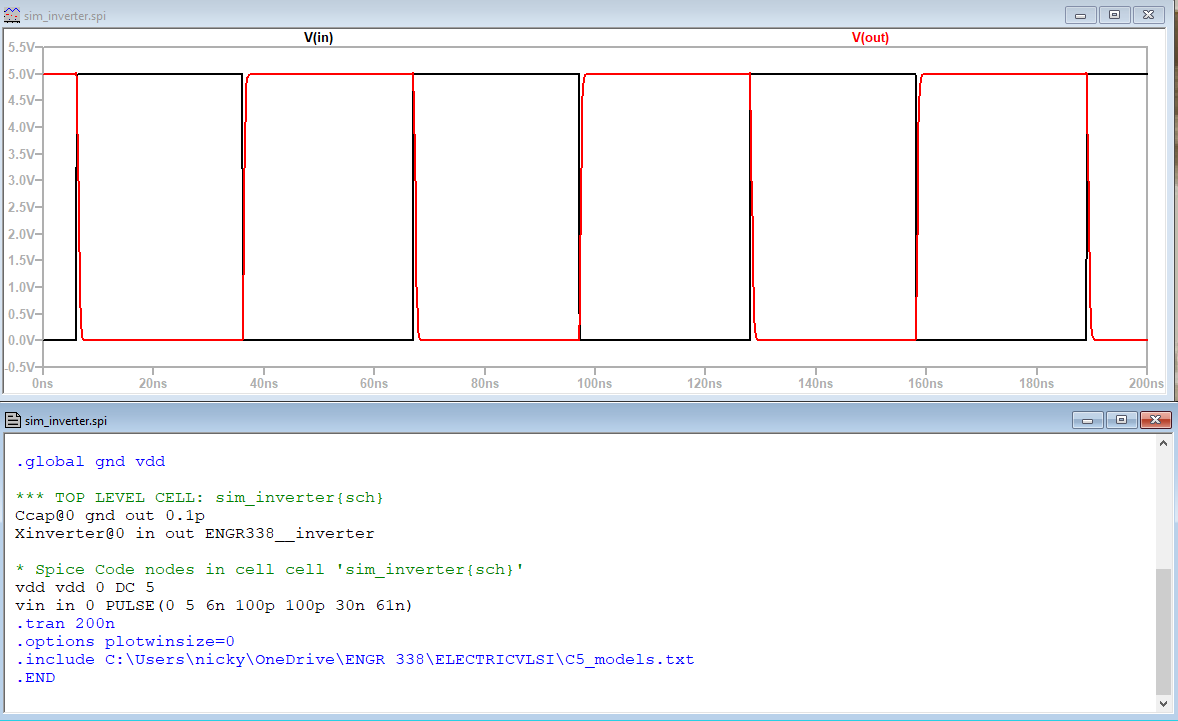
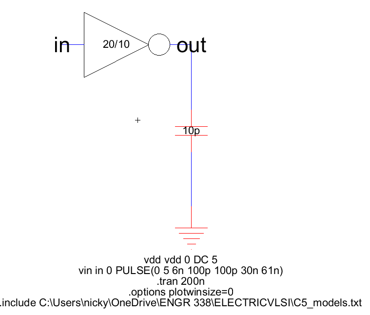
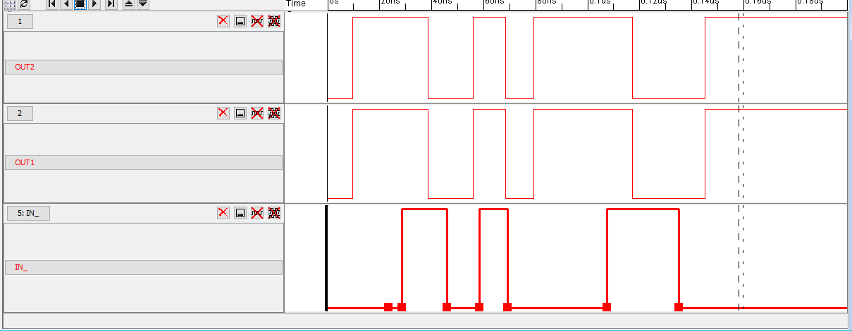
Figure 5. A simulation schematic was created for the 20/10 inverter, The simulation above shows the simulation of the inverter with a capacitor load of 100fF.
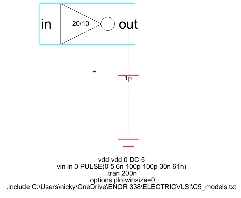
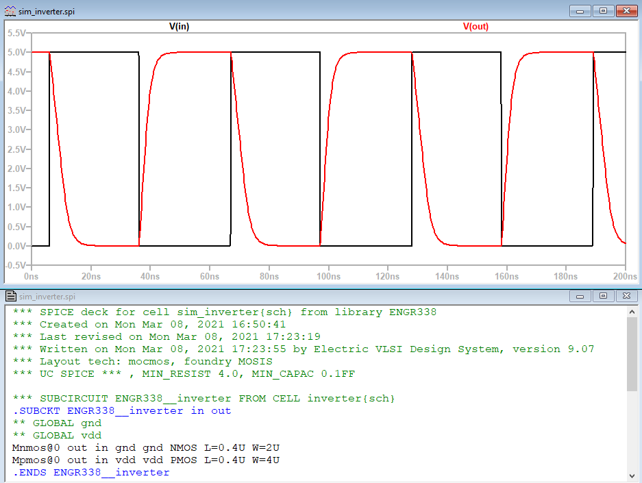
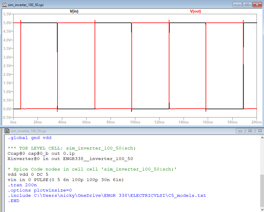
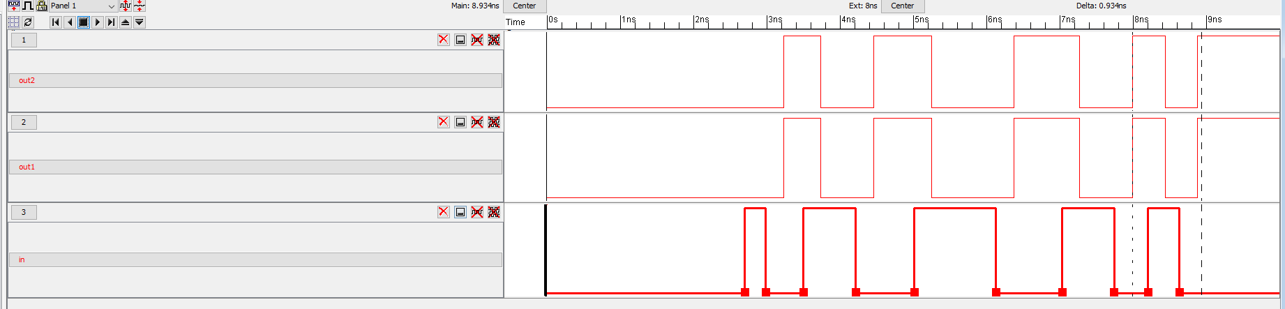
Figure 6. The same 20/10 inverter was used to simulate the inverter with a 1pF capacitor load. little error is noted to drive the full voltage.