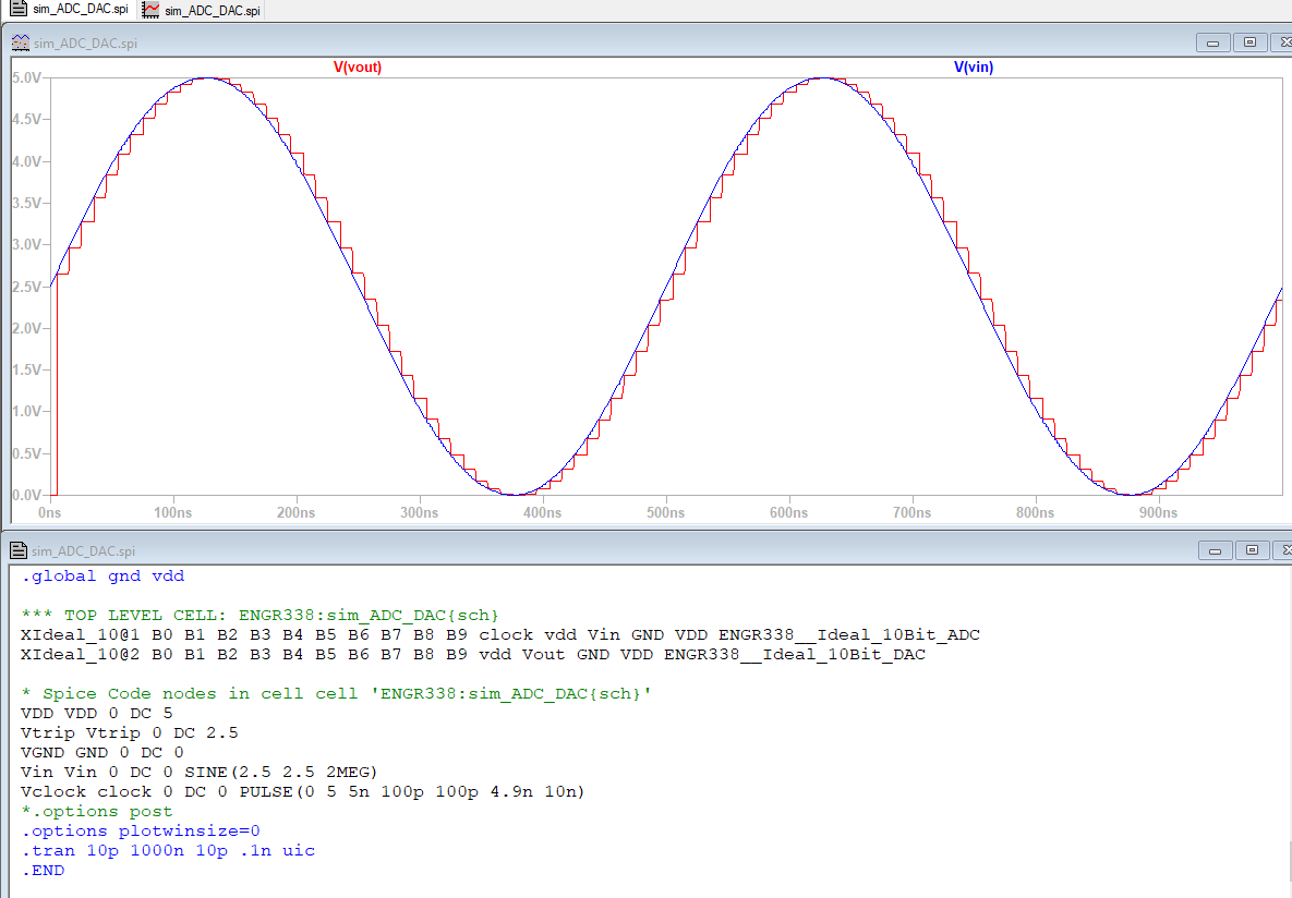
Figure 1. After downloading and using the provided ideal ADC_DAC sch, a simultation was created on LTSpice to display a discrete signal to track the analog sine wave from vin.
Task 2
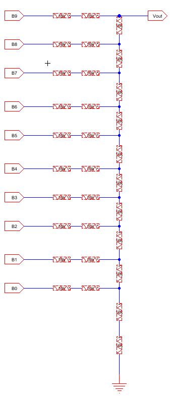
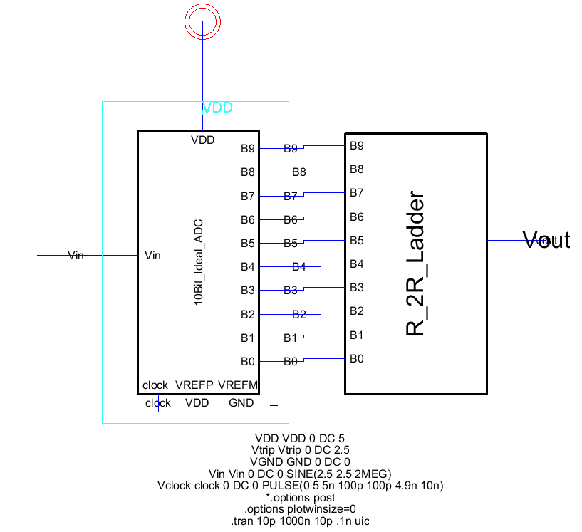
Figure 2. Figures above show the R_2R Ladder built along with the schematic where it is connected to the ideal ADC.
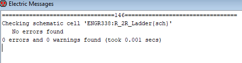
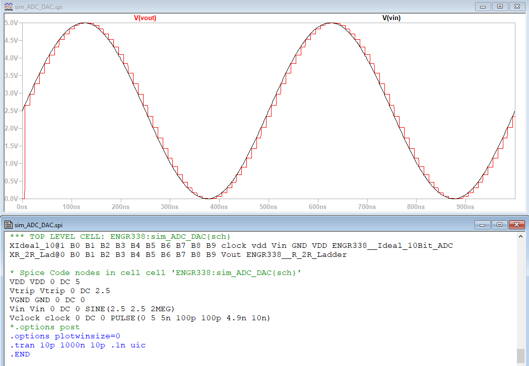
Figure 3. Figures above show a DRC check from Electric VLSI showing no errors, The schematic was sent to LTSpice to do the simulation of the newly made schematic.
Figure 2. Figures above show the R_2R Ladder built along with the schematic where it is connected to the ideal ADC.
Figure 3. Figures above show a DRC check from Electric VLSI showing no errors, The schematic was sent to LTSpice to do the simulation of the newly made schematic.
Task 3
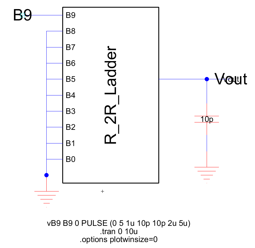
Figure 4. New schematic using the R_2R_Ladder, pins B0-B8 where grounded and B9 was connected to a Pulse. a 10pF capacitor was added as a load to check for time delay.
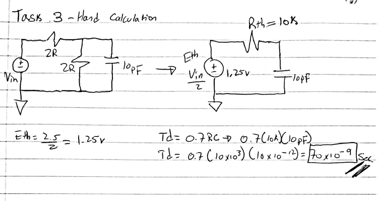
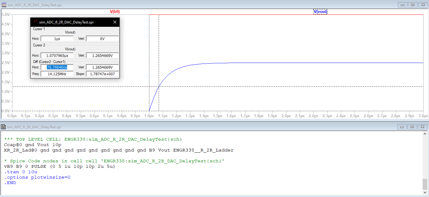
Figure 5. Left image shows hand calculation of the RC circuit transformed into a Thevenin's Equivalent circuit and calculation of time delay. Second image shows the simulation in LTSpice confirming the time delay.
Figure 4. New schematic using the R_2R_Ladder, pins B0-B8 where grounded and B9 was connected to a Pulse. a 10pF capacitor was added as a load to check for time delay.
Figure 5. Left image shows hand calculation of the RC circuit transformed into a Thevenin's Equivalent circuit and calculation of time delay. Second image shows the simulation in LTSpice confirming the time delay.