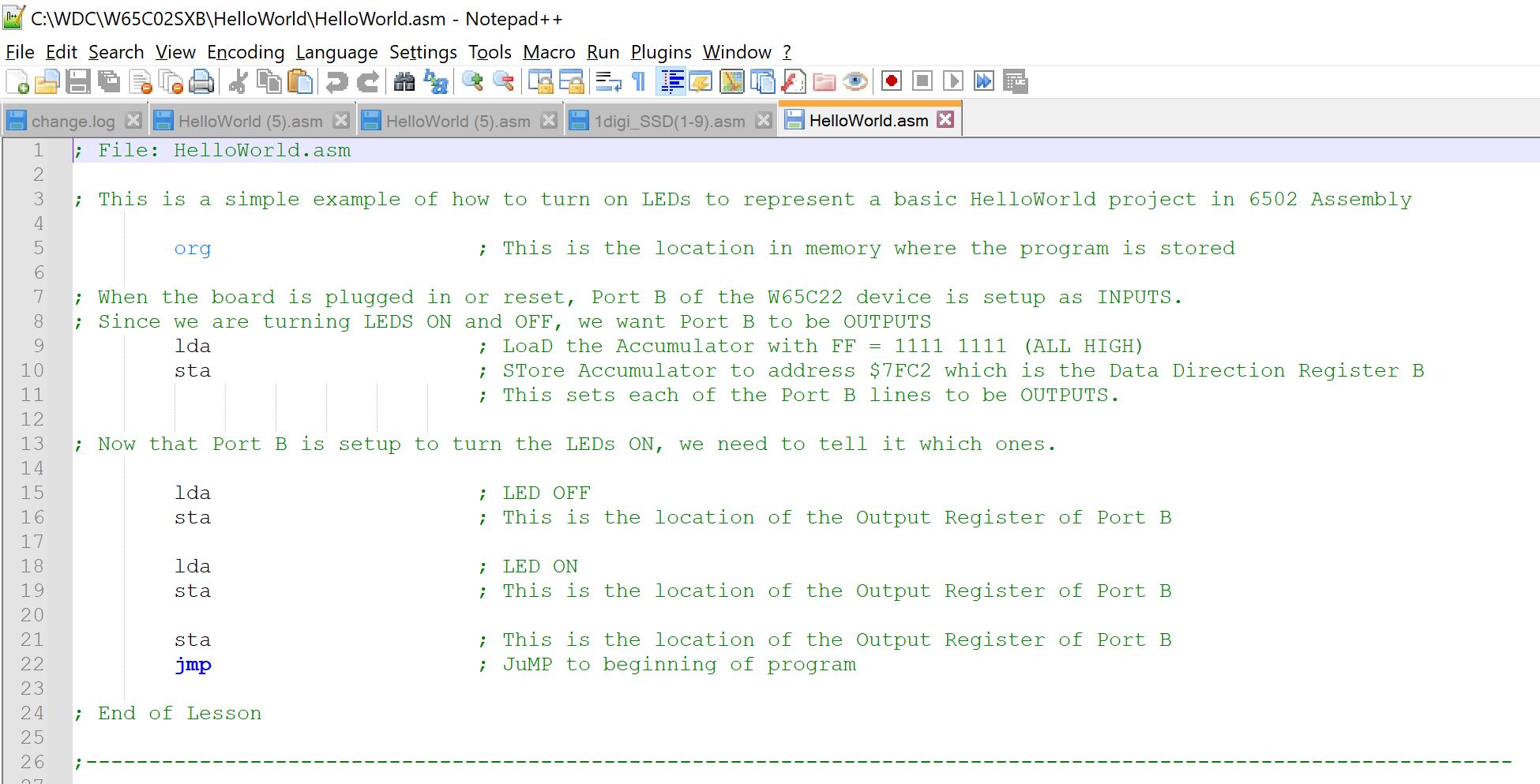
To start, go into your newly created WDC folder where you extracted the github project and move into the W65C02SXB folder. The folder should have the HelloWorld project folder and the W65C02S_Demo folder. Move into the HelloWorld folder and open HelloWorld.asm with a text editor of your choice. In this tutorial, I am using Notepad++, which is shown below:
This 6502 assembly code above was written by David Gray, an engineer at WDC. You can find the full 6502 instruction set here. Whats great about 6502 is that there is only about 50 instructions, so one can realistically understand the entirety of the instruction set and therefore understand what is really happening inside the processor.
To start, we will define the memory addresses of the 6522 VIA's as variables. These are the locations in the memory that point to the registers we want to access. The base memory address for the 6522 VIA is $7FC0 and the other I/O pins are the next sequential addresses.
VIA_BASE_ADR: EQU $7FC0 ; (Base address of the 6522 VIA.) Makes VIA_BASE_ADR EQUivalent to the memory location $7FC0
PB: EQU VIA_BASE_ADR+0 ; Addresses of registers in 6522.
PA: EQU VIA_BASE_ADR+1
DDRB: EQU VIA_BASE_ADR+2
DDRA: EQU VIA_BASE_ADR+3
We begin by defining a location in the memory where the program we are writing can be stored. $1900 is a good spot. So our first instruction is org $1900. This tells the assembler to ORiGinate the following instructions after the $1900 location in the memory.
To output through port B, we must first configure the data direction register to output. When the DDR is low, it is an input. When it is high, it is an output. To do this for port B, we want to store a value of FF (high) into the DDRB register. This is shown below:
lda #$FF ; LoaD the Accumulator with FF = 1111 1111 (ALL HIGH)
sta DDRB ; STore Accumulator to address $7FC2 which is the Data Direction Register B
; This sets each of the Port B lines to be OUTPUTS.
The # denotes an explicit value to be loaded. If you did not include the #, the MPU would think we want to load from memory location $FF. Now, Port B is configured as an output and we can load different values to output throught it.
To blink the LED, we want it to be low then high or vice versa.
lda #$00 ; LED OFF
sta PB ; This is the location of the Output Register of Port B
jsr DELAY
lda #$FF ; LED ON
sta PB ; This is the location of the Output Register of Port B
jsr DELAY
jmp $1900 ; JuMP to beginning of program
Here, the jsr instruction tells the MPU to jump to the DELAY subroutine. This is a secondary section of code created by David Gray which simply delays the MPU for 65535 cycles then jumps back to where it left off. This allows us to see the LED blinking. Without it, the blinking would be to fast for us humans to recognize. The DELAY subroutine is given below. Add it too your code.
DELAY:
phx
phy
ldy #$00
?L2 ldx #$00
?L1 dex
bne ?L1
dey
bne ?L2
ply
plx
rts
That is it for our blinking code. We can now upload it too the board. To do so, open the tide application in the WDC/Tools/Bin folder. Click file, open project. Navigate back to the HelloWorld folder and open the HelloWorld.wdc file. An error will show, but this is okay. Click through. Now click the compile button circled in yellow below.
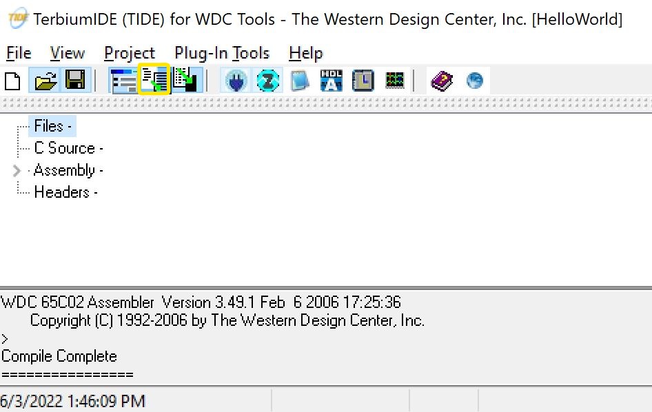
Make sure there are no errors in the text box below, then click the button to the right of the compile button to assemble and link the compiled code. The assembler converts our 6052 assembly code into machine code, which the MPU can understand.
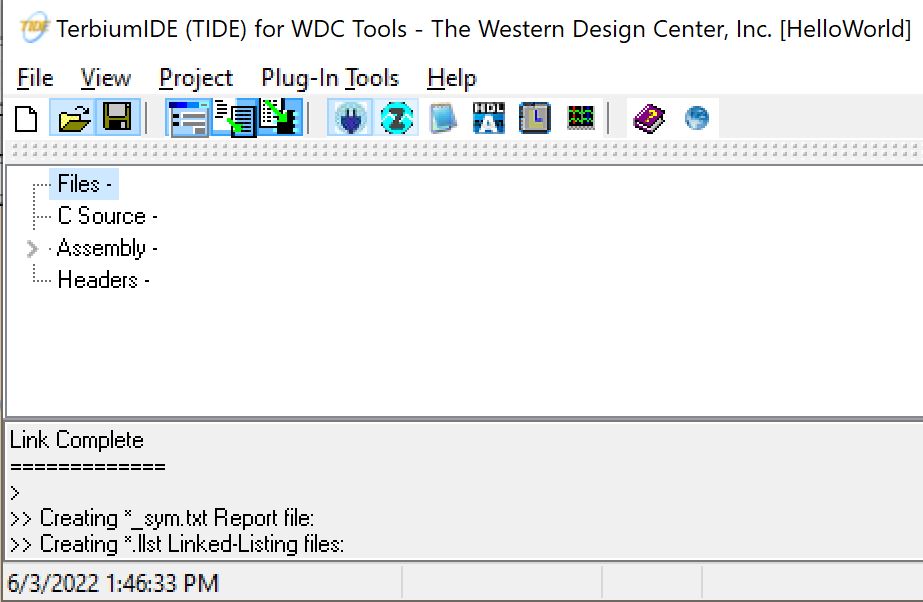
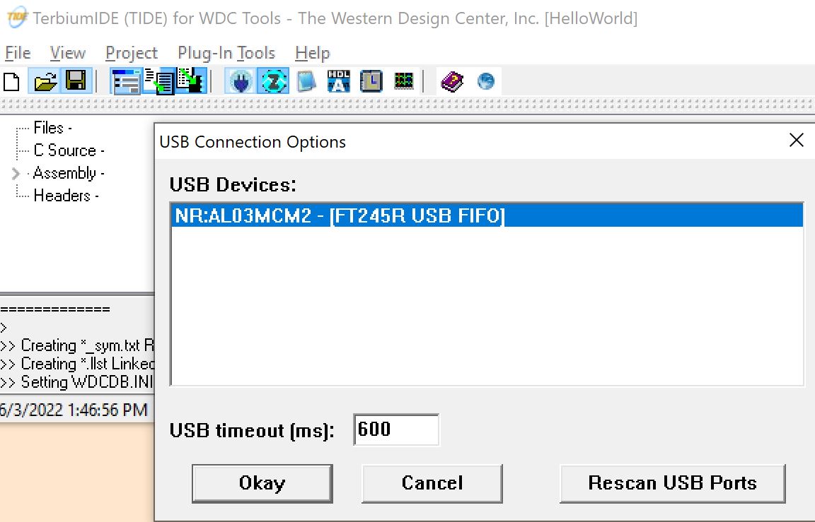
Once it says link complete, click the button with the blue Z in the circle to open the debugger. Select the USB port that your board is connected to then click okay.
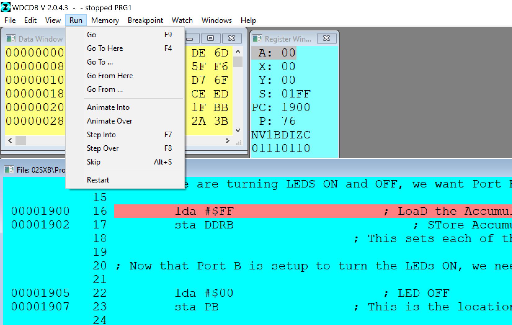
The debugger will open and your code should be loaded on the screen in blue. Now, click the run tab and then click Go as displayed below. This uploads the machine code to the MPU.
The code will then be uploaded to the board. Plug an LED in as we did in the previous tutorial and we will see it blinking. This is demonstrated below.
If there are any questions or comments, feel free to email me at mtkrauss@fortlewis.edu
In the next tutorial, we will implement a 8 bit binary counter that is displayed on external LEDs.