CE 433 Report 4
Datatypes
Name: Max Krauss
Email: mtkrauss@fortlewis.edu
Data Storage Units
---------------------
1. Repeat the simulation in Sections 1 - 3. (20 points)
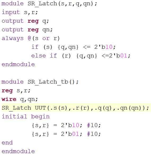
Figure
1: Verilog Code for SR Latch.
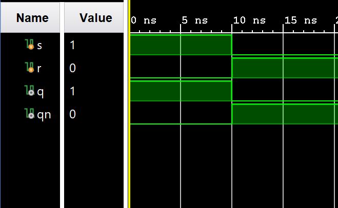
Figure 1.1: Vivado Simulation for SR Latch.
--------------------------------------------------------------------------------------------------------------------------------------------
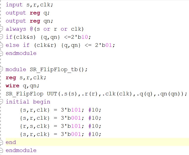
Figure
2: Verilog Code for SR Flip-Flop
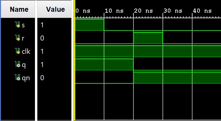
Figure 2.1: Vivado simulation for SR
Flip-Flop
--------------------------------------------------------------------------------------------------------------------------------------------
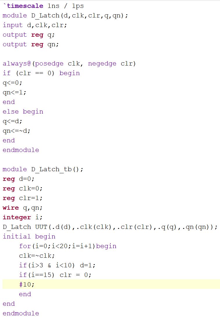
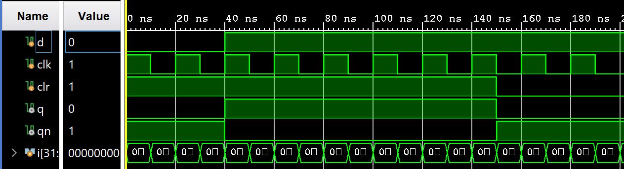
Figure 3: Verilog code for Edge Triggered D Flip-flop. Figure 3.1: Vivado simulation for Edge Triggered D Flip-flop.
--------------------------------------------------------------------------------------------------------------------------------------------
2. Write the testbenches and run simulations for Section 4 and Section 5. (20 points)
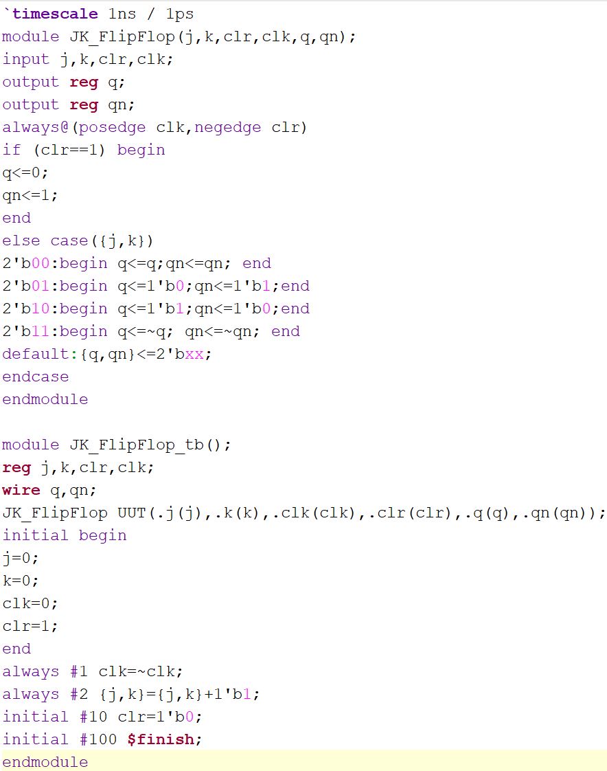
Figure
4: Verilog code for JK Flip-Flop w/ testbench.
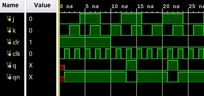
Figure 4.1:
Vivado simulation for JK Flip-Flop.
--------------------------------------------------------------------------------------------------------------------------------------------
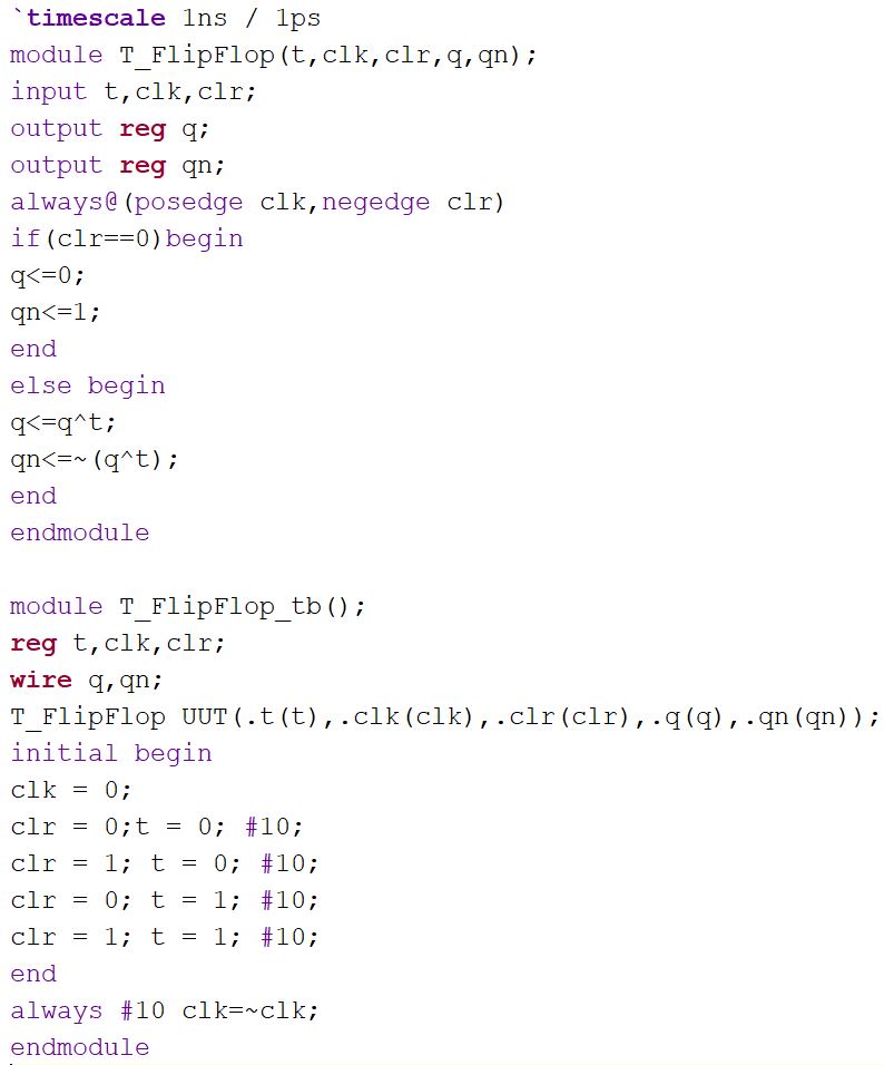
Figure
5: Verilog code for T Flip-Flop with testbench.
Figure 5.1: Vivado simulation for T
Flip-Flop.
--------------------------------------------------------------------------------------------------------------------------------------------
3. Repeat all the work in Section 8 and complete the task described in the end of Section 8. (60 points)
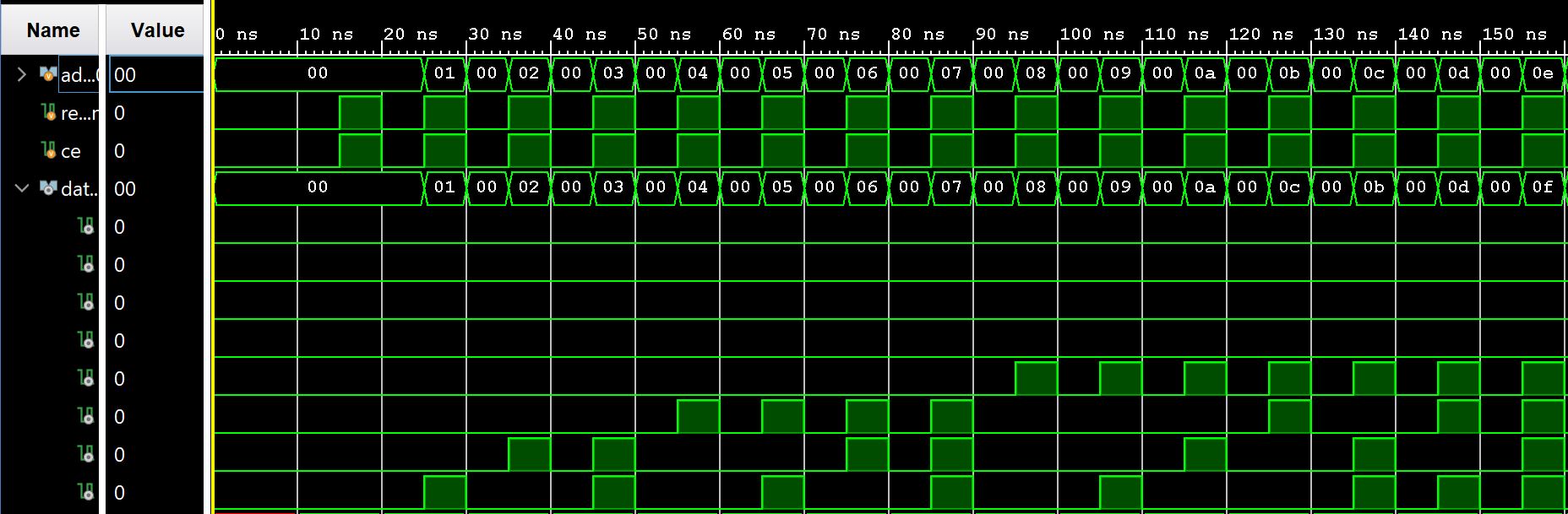
Figure 6: Vivado simulation for the binary ROM.
--------------------------------------------------------------------------------------------------------------------------------------------
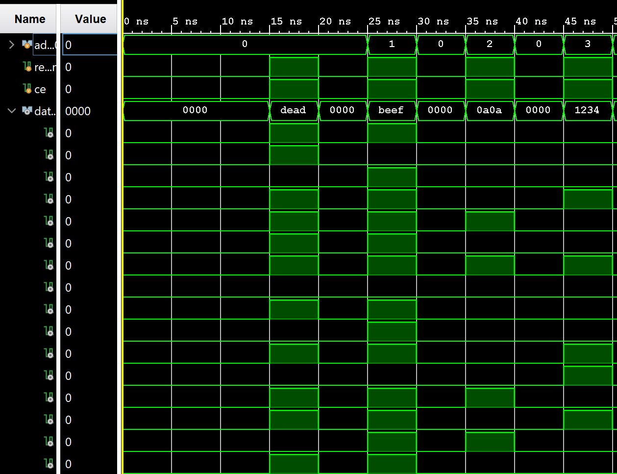
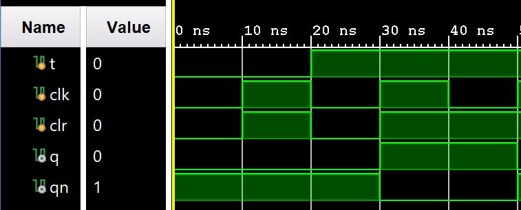
Figure 7: Vivado simulation for the hex ROM.
--------------------------------------------------------------------------------------------------------------------------------------------
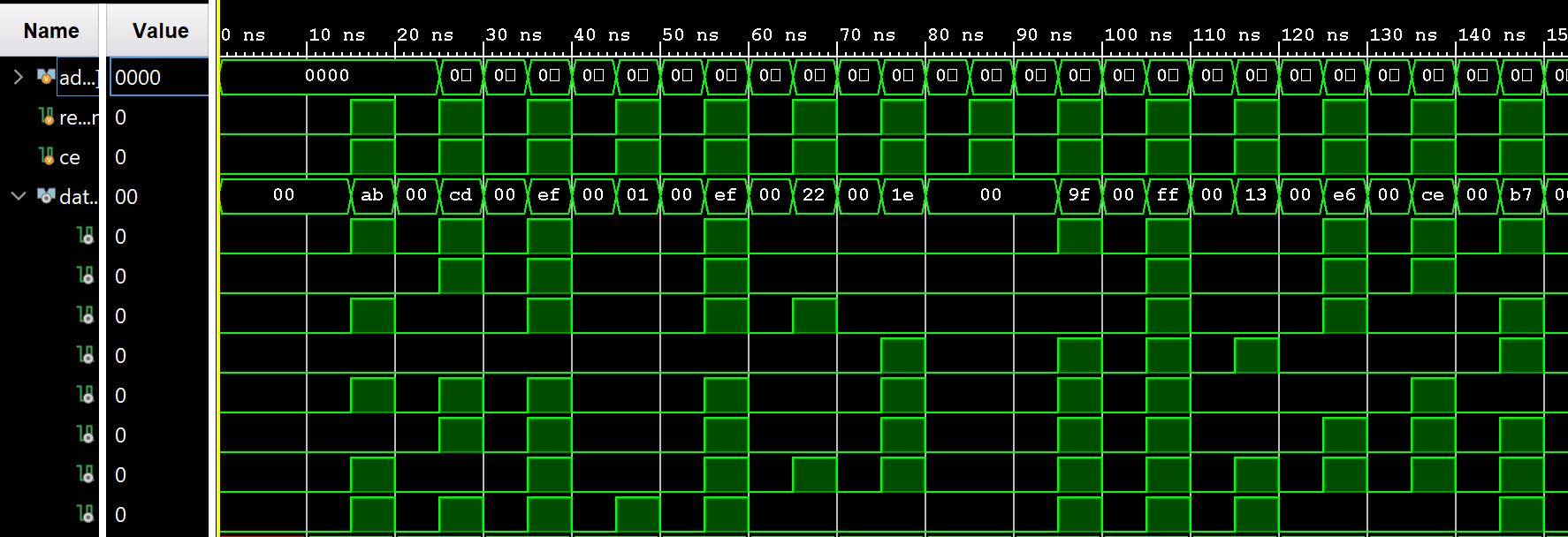
Figure 8: Vivado simulation for the 8-bit spaced hex ROM.
--------------------------------------------------------------------------------------------------------------------------------------------
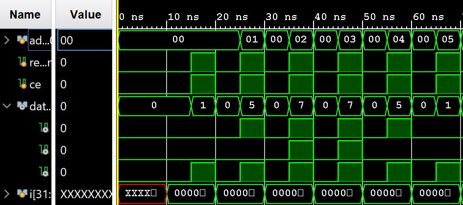
Figure 9: Vivado simulation for the 3-bit binary ROM.
--------------------------------------------------------------------------------------------------------------------------------------------
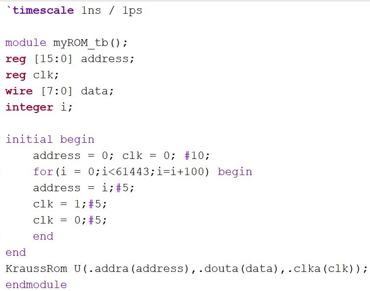
Figure 10: Verilog testbench for extraction from Vivado IP block, KraussRom.
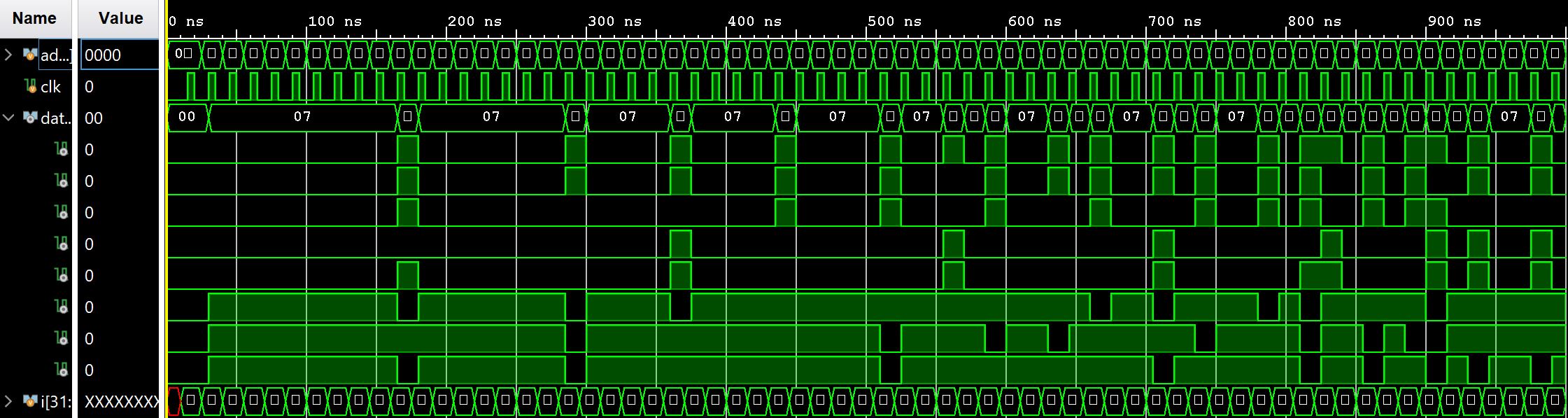
Figure 10.1: Vivado simulation for the IP block extraction.
--------------------------------------------------------------------------------------------------------------------------------------------
Results:
This tutorial taught us how data storage units are designed and
allowed us to view how they work in Vivado simulations.