CE 433
Lab 3 - More FPGA Max Krauss
mtkrauss@fortlewis.edu
The purpose of this lab is to practice combinational logic
by programming FPGA's using Verilog and Vivado. We also learned how to
use the SSD on our FPGA.
Materials: Baysys3, Vivado, USB-C, and a personal
computing device for photo/video results. 1.
Using Verilog and Vivado to demonstrate the following combinational
logic blocks in both simulation and on the board (switches/leds): 1)
Inverter
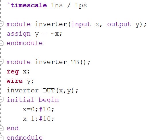
Figure 1.1: Verilog code for the Inverter w/ testbench. Figure 1.2:
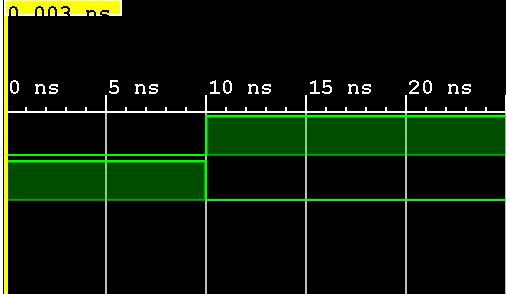
Vivado simulation for the inverter.
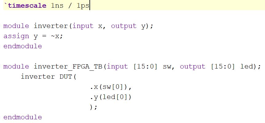
Figure 1.3: Verilog code for the FPGA testbench.
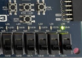
Figure 1.4: On-board verification of the inverter.
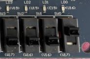
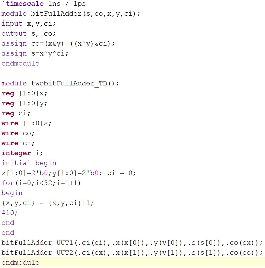
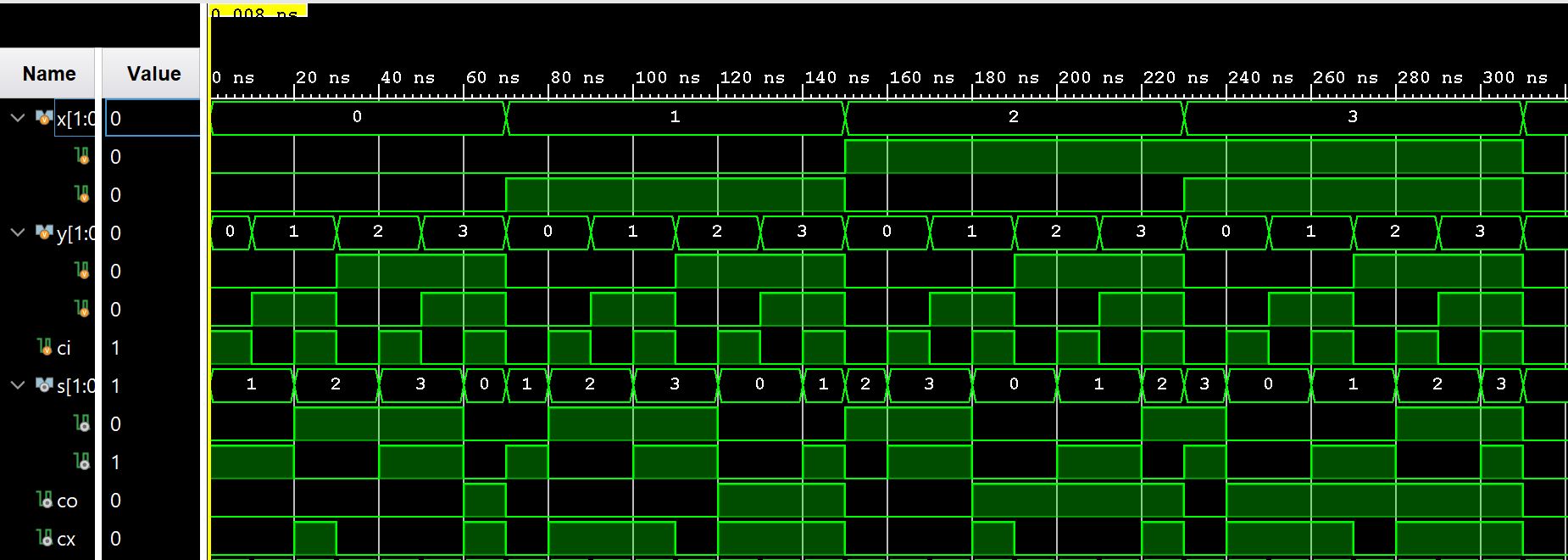
2) 2-bit full adder Figure
2.1: Verilog code for the 2-bit FA
Figure 2.2: Vivado simulation for the 2-bit FA
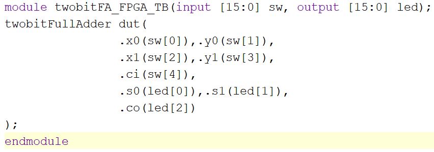
Figure 2.3: Verilog code for the FPGA testbench.
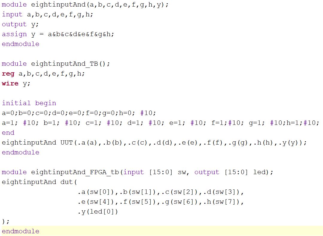
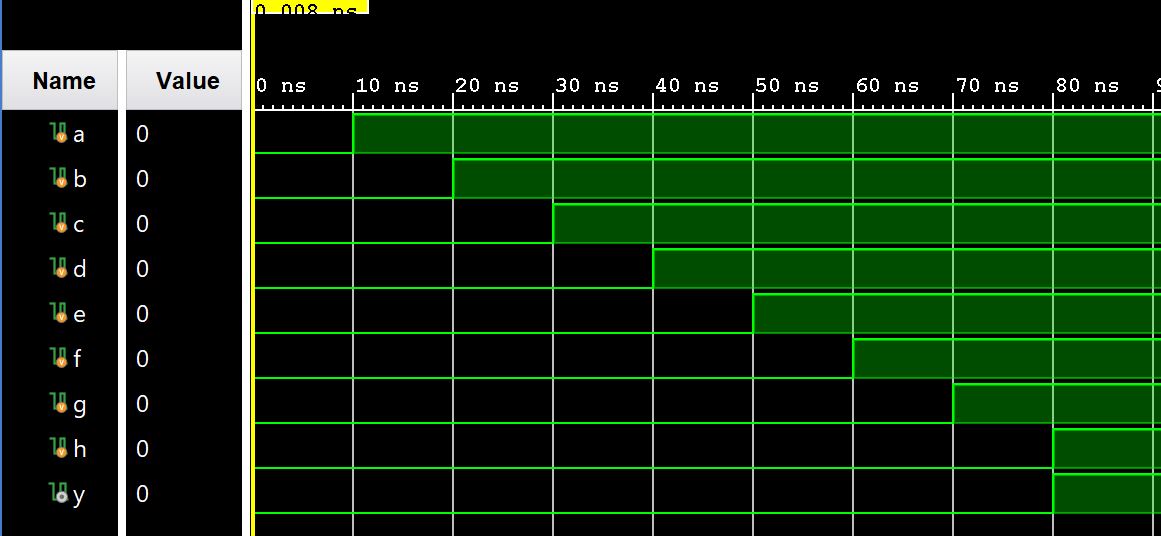
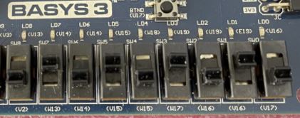
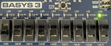
3) 8-input And
Figure 3.1: Verilog code for the 8-input And gate.
Figure 3.2: Vivado simulation for the
8-input And gate.
Figure 3.3: On-board verification for the 8-input And gate.
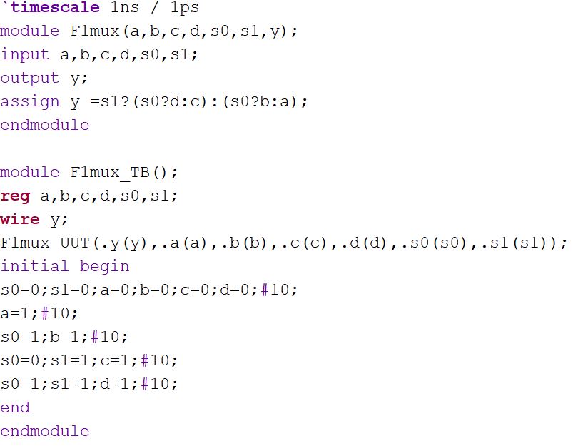
4) 4-1 MUX Figure
4.1: Verilog code for 4-1 MUX.Figure
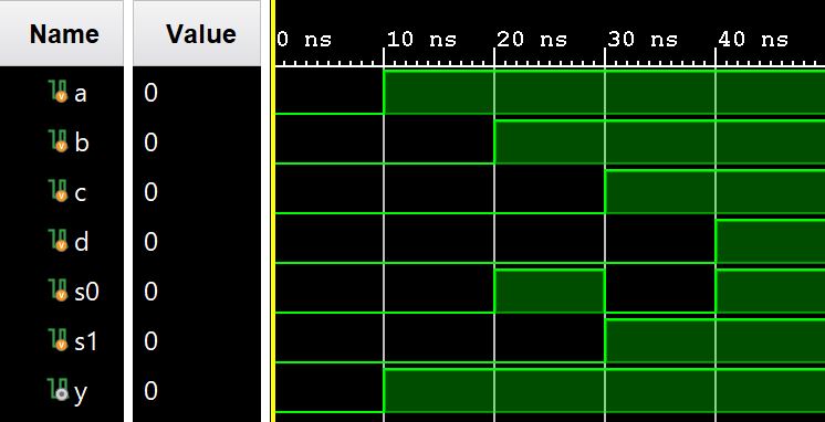
4.2: Vivado simulation for the 4-1 MUX.
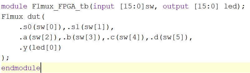
Figure 4.3: Verilog code for 4-1 MUX FPGA testbench.
2.
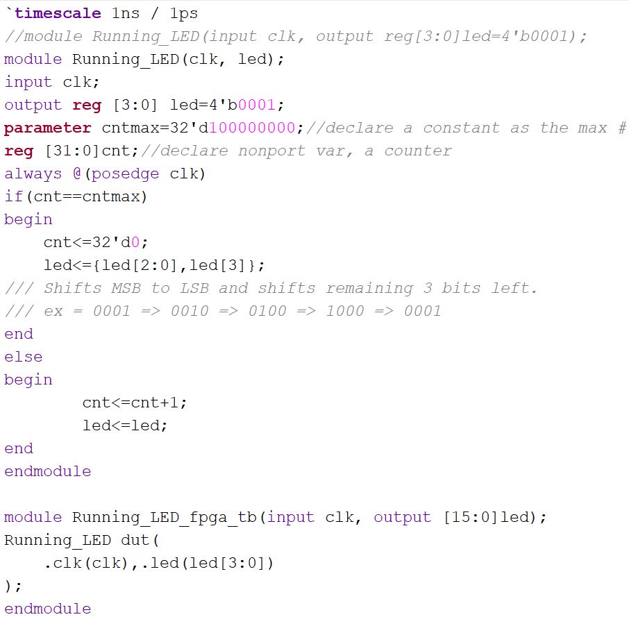
Using Verilog and Vivado to design a 'Running LED' program on the FPGA
board. Use 4 LEDs on the board, turn on each of them for 1 second
one-by-one.
Figure 5: Verilog code for the Running LEDs.
3.
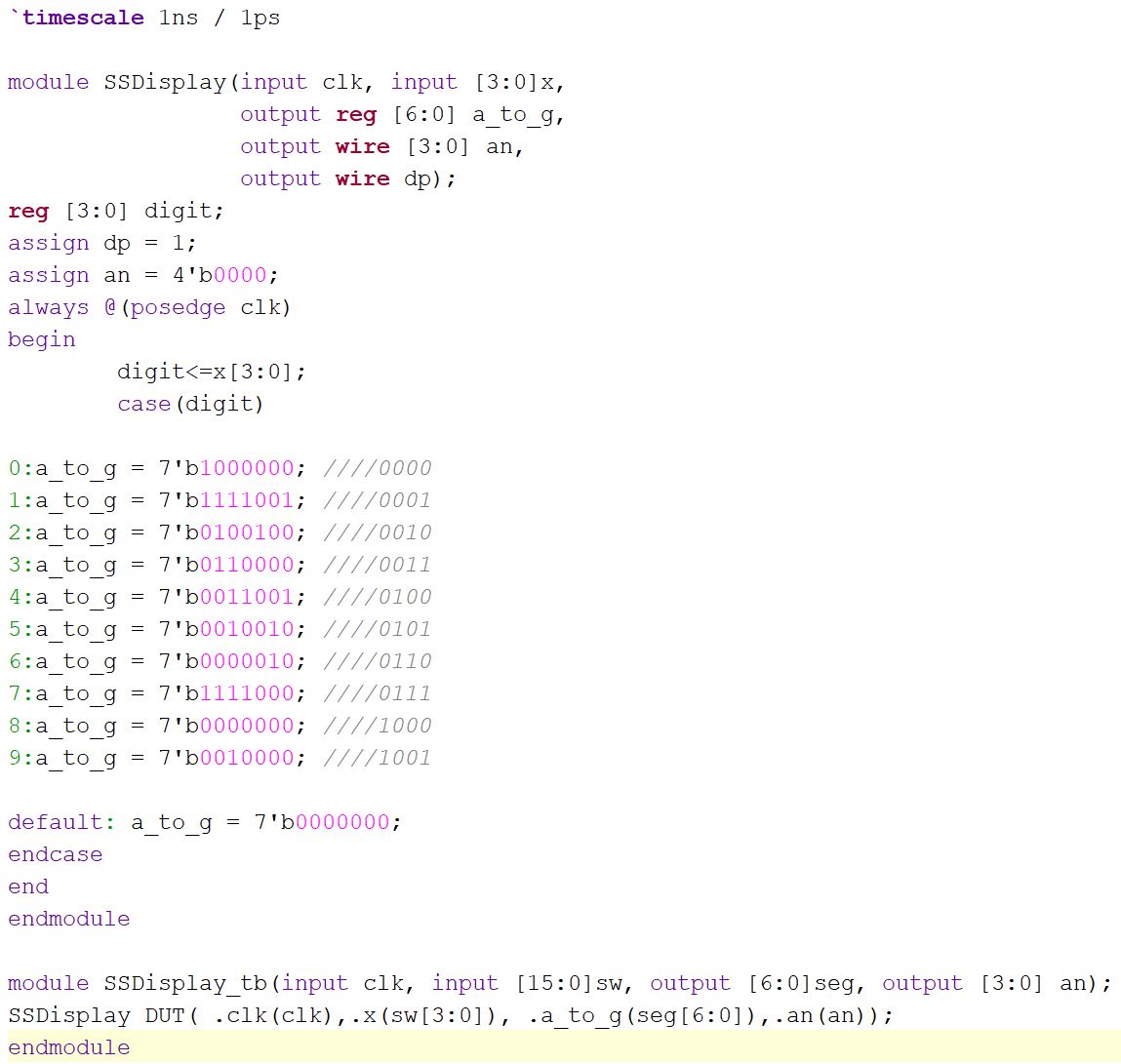
Interface the switches with the 7-segment display on the board. (make
sure you have the '##7 segment display' part in your constraint file
uncommented) The
final result should show numbers 0-9.
sw[3:0] provide binary inputs and the 4 7-segment display show the
corresponding decimal numbers.
Figure 6: Verilog code for the SSD on the FPGA.
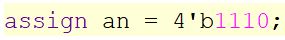
4.
Modify the code, disable any 3 of the 7-segment displays and only show
the number on one of the displays.
Figure
7: Code snippet for the one change needed to make the modification in
task 4.
Results:
This lab gave us more tasks that allowed us to practice coding
combinational blocks and implementing them on FPGAs. I had some
complications with understanding the implementation of the last three
tasks, but Doctor Li was able to clarify the confusions I had.