1 A Outputs
Our first power module was created to transform our input power into 5V and 3.3V with a 1A current. To do so, I wired up two 1117 voltage regulators, a 1N4007 diode, two 0.1uF caps, a 1uF cap, a 10uF cap, an LED, a 470 ohm resistor, and a ground. The output after the first regulator was pinned to the 5V_1A power out pin and the output after the second was pinned to the 3.3V_1A power out pin. This module is displayed below in figure 1.
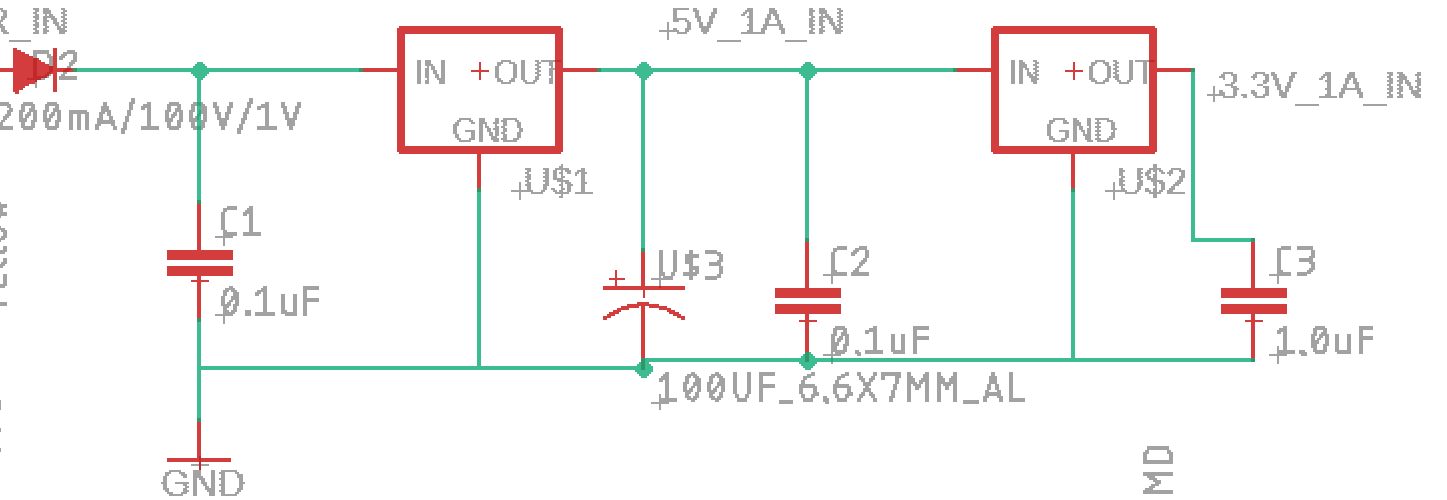
Figure 1: 1A Power Module
3 A Outputs
For the second and third power module, we needed to output 3A with both 5V and 3.3V. To do so, both modules utilized a 4.7uF cap, a ground, Schottky diodes, and LM2596 power converters. The Schottky diodes and LM2596 were not provided in Eagle's or Sparkfun's library, so I recreated them in my personal eagle library.
The footprint for both the Schottky diode and the LM2596 are displayed below in figure 2 and 3. The 5V_3A module also included a 47uH inductor and a 22uF cap in its design, whereas the 3.3V_3A module contains a 33uH inductor and a 33uF cap in its circuit. Each output was pinned to its corresponding power out pin in the schematic.
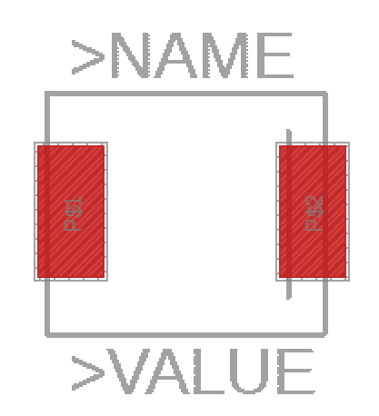
Figure 2: Footprint for the Schottky Diode
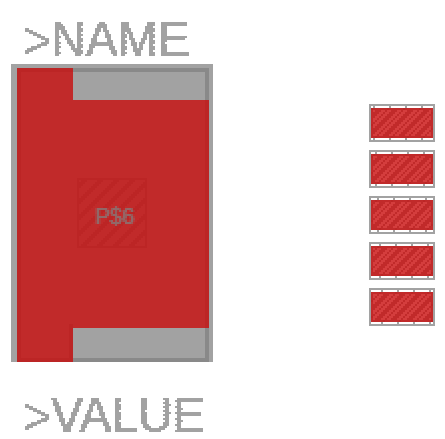
Figure 3: Footprint for the LM2596 Power Converter
The final schematic for my power supply circuit is displayed below in figure 4. The 2 sets of 6 pins are designed to allow the user to choose which power output is needed and then supply that output directly into the breadboard. Also, a switch was added to the power in to allow the flow of power through the modules to be cut off when the user is selecting his desired output.
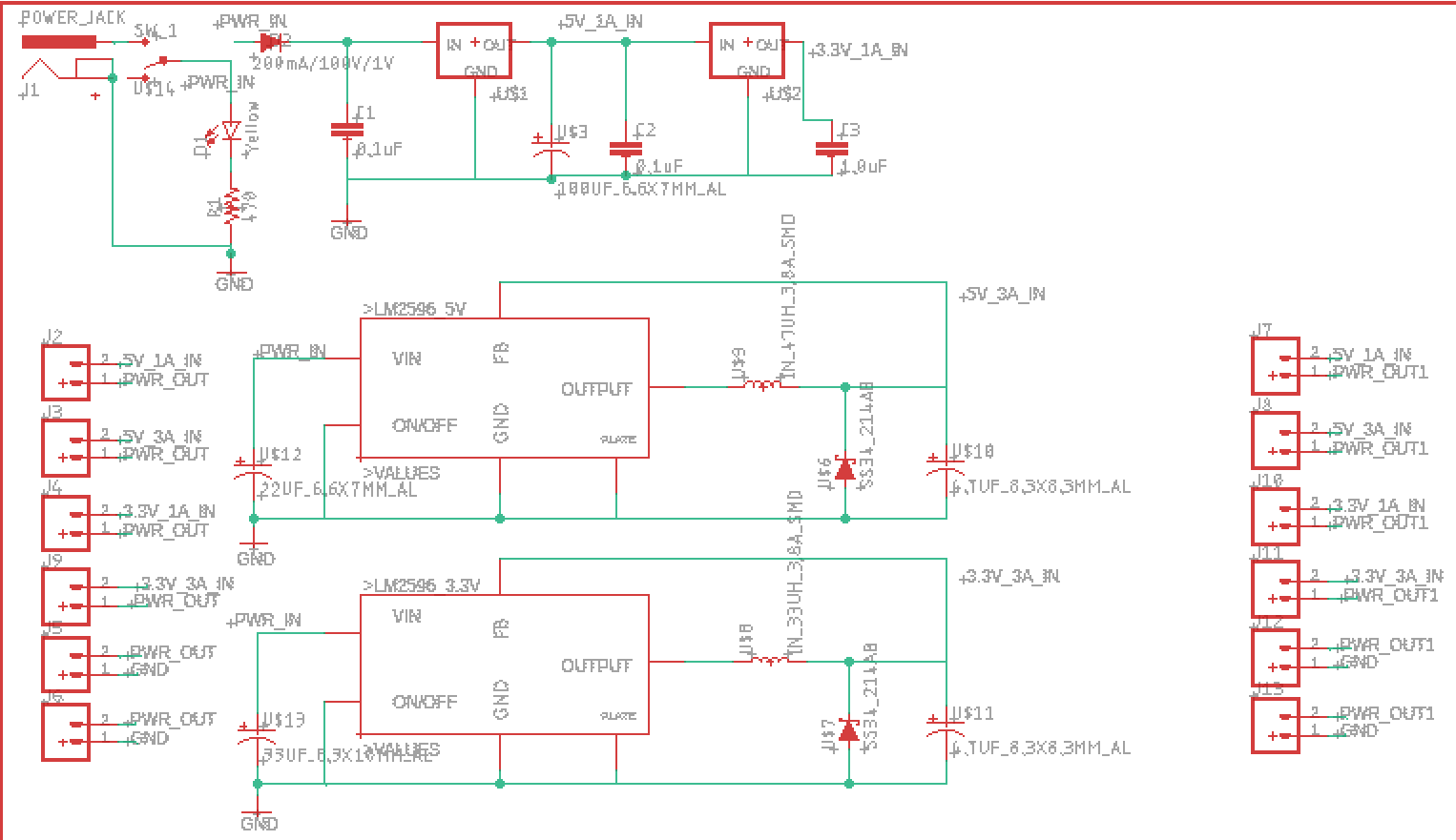
Figure 4: Power Supply Circuit Schematic
Using Eagle PCB, the schematic is converted into a board where one can then dimension the inputs and output to their liking. For this design, we needed the whole board to be able to fit onto a breadboard about 53.5 mm wide. Also, the power out pins need to be dimensioned correctly in order to fit comfortably on the rails of the breadboard with equal weight distribution so the board does not bend. To correctly dimension the output pins, I used digital calipers to measure the pin holes position on the breadboard and then placed them accordingly. The final board schematic and silk-screen layer are displayed below in figures 5 and 6.
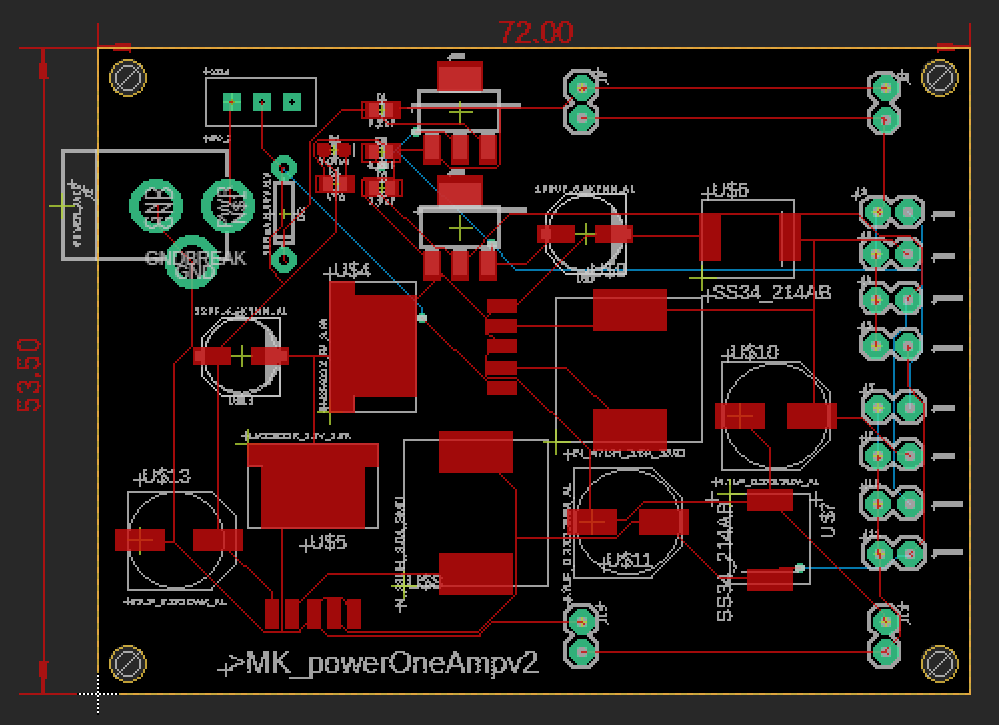
Figure 5: PCB Layout for Power Supply Circuit
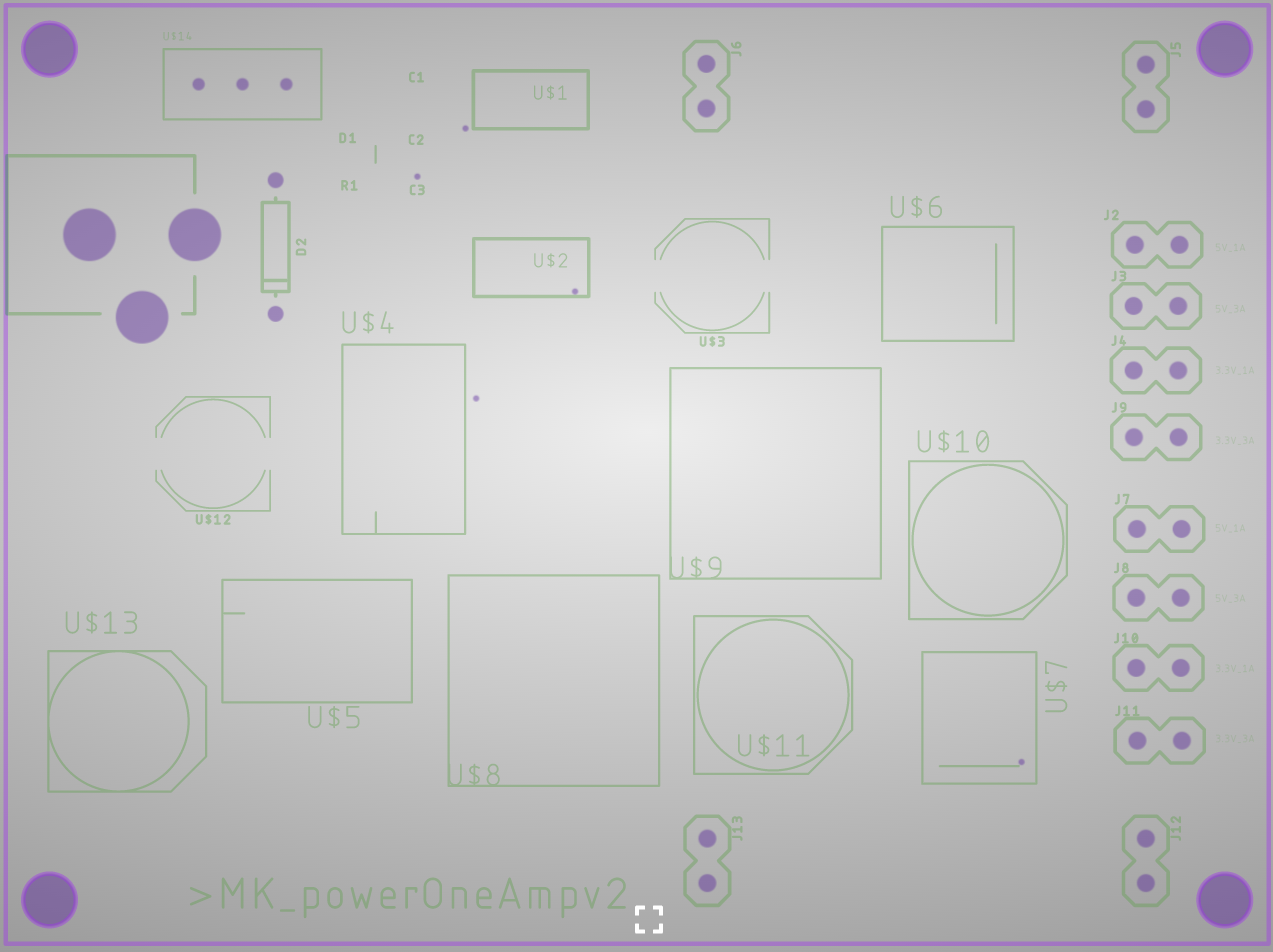
Figure 6: Silkscreen layer of the PCB. Choice pins are labeled, just very hard to see since they are only 0.5mm
Once the components are wired and the copper is virtually poured on both sides, it is ready for fabrication. This task was a perfect intro to the world of PCB maufacturing. While intricate and time consuming, this project allowed me to understand PCB work flow in the real world from idea, to schematic, to board. Even though this is a simple device, the design and concept in whole can become convoluted quickly as there is tons of minute details that can be overlooked. Completing this assignment is just like opening the door into a new, exciting, and seemingly infinte concentration of computer engineering.