ENGR338 Lab 2021 Spring
Lab 6 Build a NAND, NOR, XOR, and Full Adder
Name: Keon Nez
Email: ktnez@fortlewis.edu
Build a NAND, NOR, XOR, and Full Adder
Introduction
The Electric VLSI Design system is an EDA tool. Electric is used
to draw schematics and to do integrated circuit layout. It can also
handle hardware description languages such as VHDL and Verilog. Also
the Electric VLSI tutorial here can be used to setup the
Electric/LTSpice configuration. Using
Electric VLSI to
draw schematics and to do integrated circuit layout the schematic of an
NAND, NOR, XOR, and Full Adder. Handling hardware description languages
from the ADC-DAC
files with LTSpice and IRSIM. Familiarizing ourselves with a state of
the art computer aided design system for simulation circuit design.
Materials
- Operationg Systems: Electric and LTSpice & IRSIM
- Libraries of the ideal ADC/DAC - Found here
- Reference simulations and configurations from yilectronics.com
Methods
- Be able to layout and simulate an inverter in Electric.
-
Be able to perform simulation in both LTSpice and IRSIM.
- Design a MOSFETs in Electric.
- Understand the operation/simulations to analyse the IV curves of the MOSFETs.
Task 1: Create the
schematic and layout of the NAND gate.
Task 2: Create the schematic and layout of the NOR gate.
Task 3: Design, simulate, and layout an XOR gate.
Task 4: Design, simulate, and layout an Full Adder.
Results
Task (1)
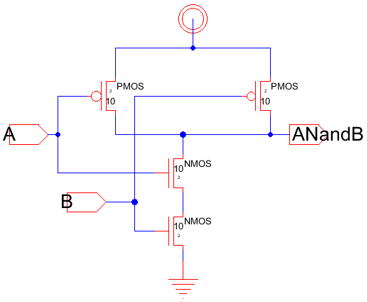 This is the schematic created for the NAND gate. In order to create a icon later.
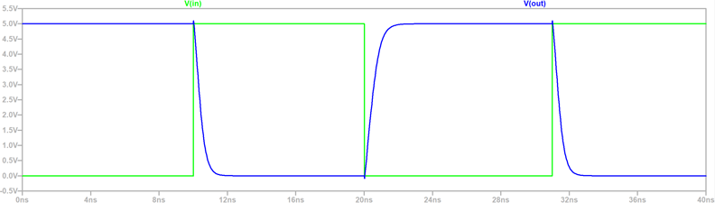 Ran the simulation prove the gate's logic.
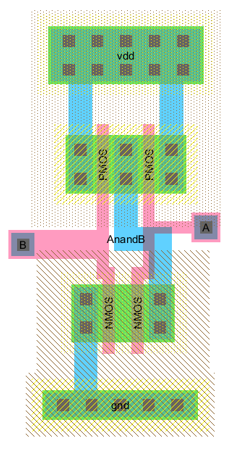 Followed the lab instuctions to create a layout in Electric.
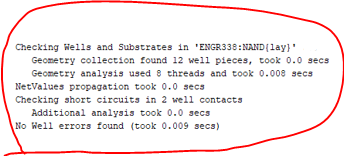 No error(s)
Task (2)
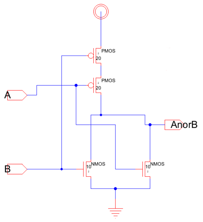
Creating the schematic of the NOR gate is similiar to the NAND gate.
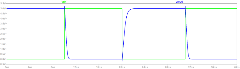
The graph from Task 1 and Task 2 are similiar in characteristics.
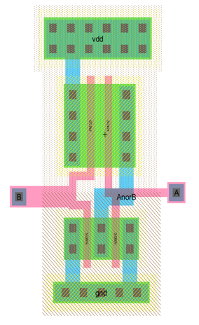
Making the NAND gate layout is simliar steps for the NOR gate's layout.
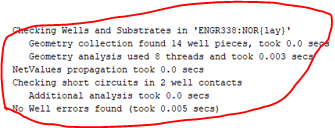
No error(s)
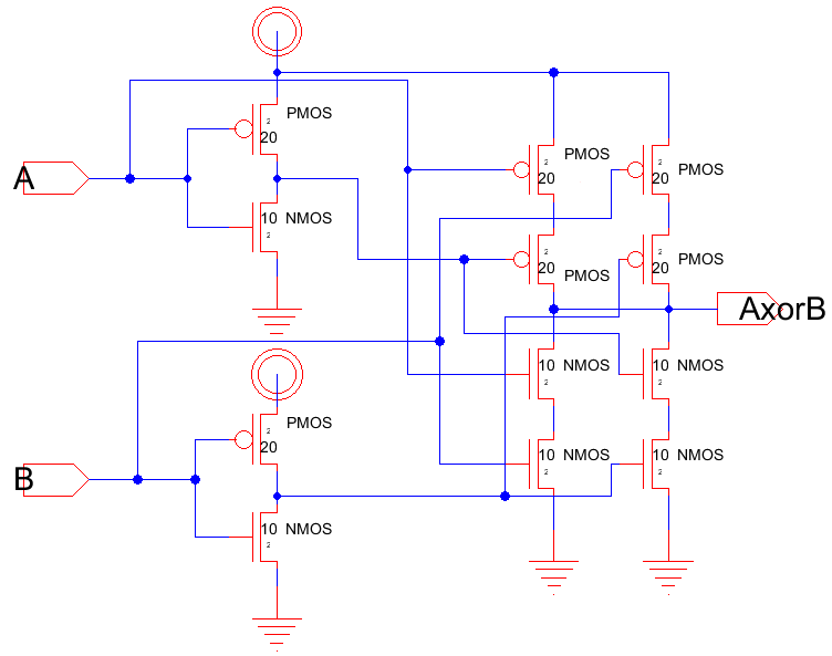
This schematic of the XOR gate had more detail to simply to a icon.
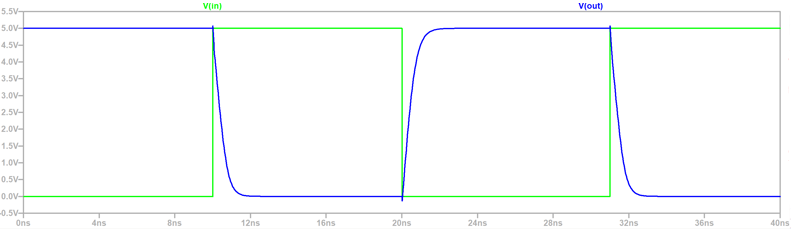
The graph does match with lab task detail provided.
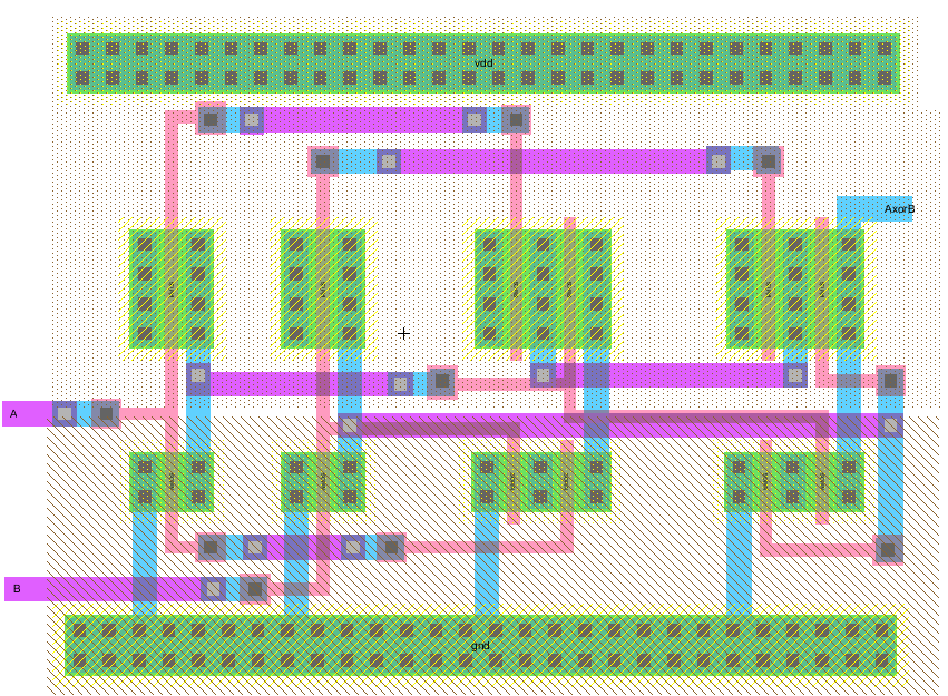
It took awhile to assemble the connections right. Using different metal layers to avoid short circuits. I couldn't use
long Poly wires which have larger resistance. Remebering that the gate should be
connected to metal for the routing.
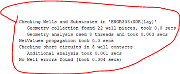
No error(s)
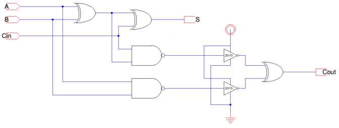
This was an easy schematic after creating the previous icons.
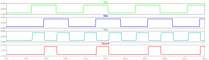
This is a Full Adder verified by logic from the graph.
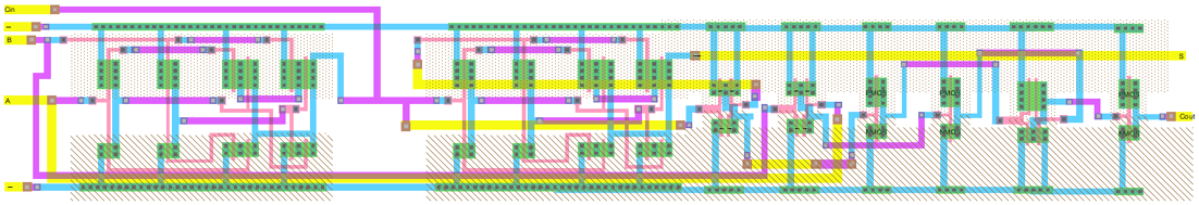
This was the longest task out of the entire lab. Having multiple layout converging together to form the final layout.
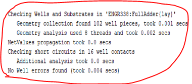
No error(s)
Discussion
A
very interesting aspect of Electric is the
ability to build similiar SPICE models of analog schematic/designs from
CE241. All the labs prior have increased my confidence working with
Electric and LTSpice.This
means I can simulate what the circuit will do for different gates of
logical or other components
operations. Although I had a tough time with the design layout of the Full Adder.