ENGR338 Lab 2021 Spring
Lab 2 Design an R-2R DAC
Name: Keon Nez
Email: ktnez@fortlewis.edu
Design an R-2R DAC
Introduction
The Electric VLSI Design system is an EDA tool. Electric is used
to draw schematics and to do integrated circuit layout. It can also
handle hardware description languages such as VHDL and Verilog. Also
the Electric VLSI tutorial here can be used to setup the
Electric/LTSpice configuration.
Materials
- Operationg Systems: Electric VLSI and LTSpice
- Libraries of the ideal ADC/DAC - Found here
Methods
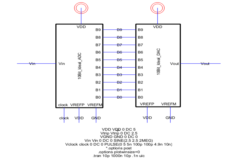
- Task 1.) Copy the existing ideal ADC-DAC files to the ENGR 338 library and run the simulation.
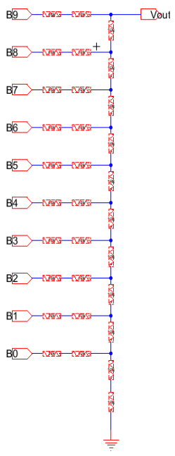
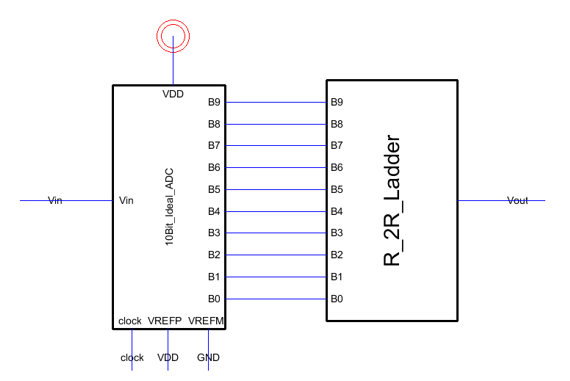
- Task 2.) Build the schematic of the R-2R DAC and the simulation.
- Task 3.) Test the time delay from the B9 pin when the DAC drives a 10 pF load.
Results
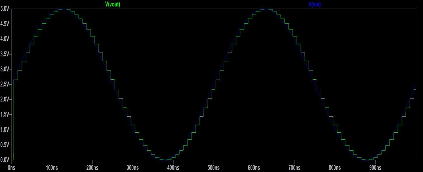
(Task 1)
(Task 2)
(Task 3)
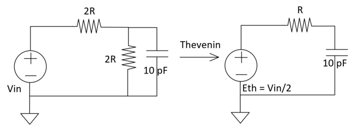
0.7*R*C = (0.7)*(10k)*(10pF) = 70ns
Couldn't finish Task 3 to simulate it and probe the time delay. V(b9)
Discussion
I understood the operation of the ideal ADC and DAC. As to the design of a R-2R DAC in Electric VLSI to replace the ideal DAC was an excellent intoduction. Overall I became familiar with Electric VLSI and LTSpice for integrated circuit
design.