Lab 3
CE 351
James Ferguson
Introduction
The goal of this lab is to become more familiar with Electric VLSI and create the schematic and layout for a 10-bit R 2R DAC using C5 technology.
Methods
The began with creating a schematic for a R 2R subsection using 10k n-well resistors with a width of 15 and a length of 187.5.
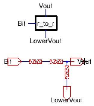
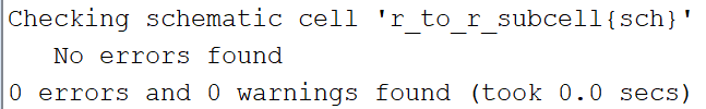
DRC error checking found nothing.
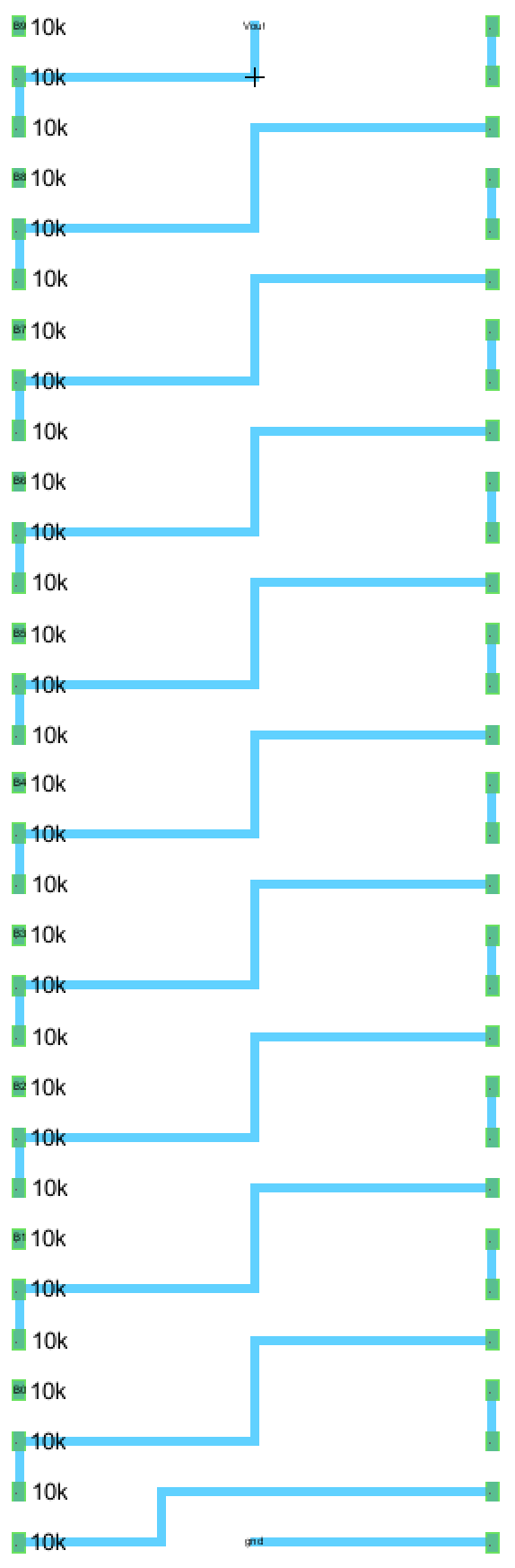
A layout was then created for the subsection.
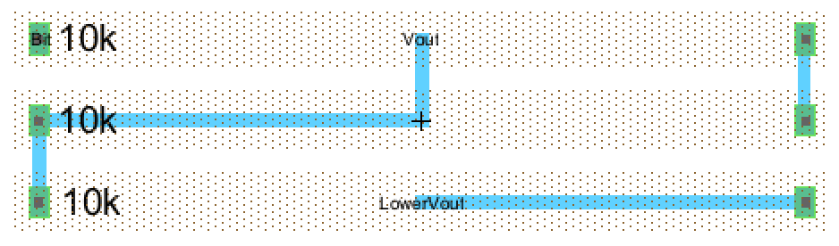
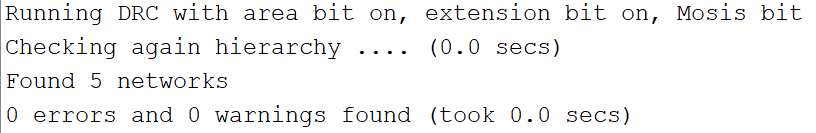
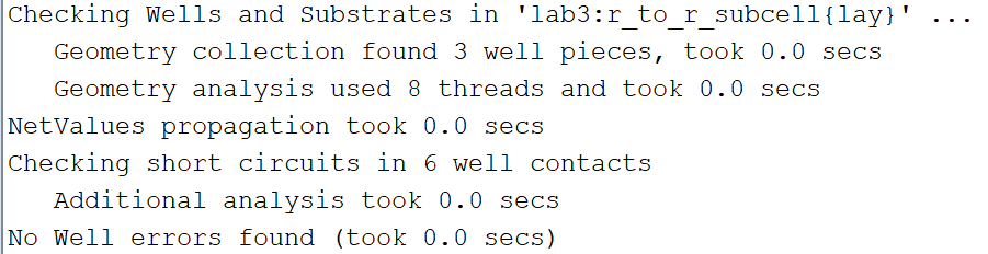
DCR, ERC and NCC where all run for the layout and returned the following.

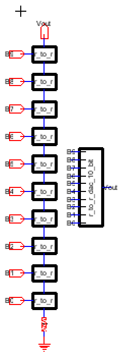
The 10-bit DAC schematic was then created using the R 2R subsections
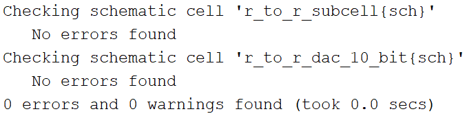
DRC error checking found nothing.
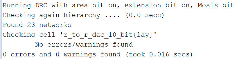
Again, the schematic was converted into a layout.
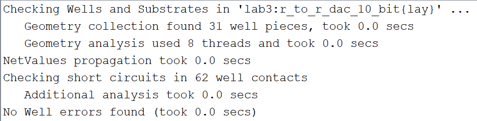
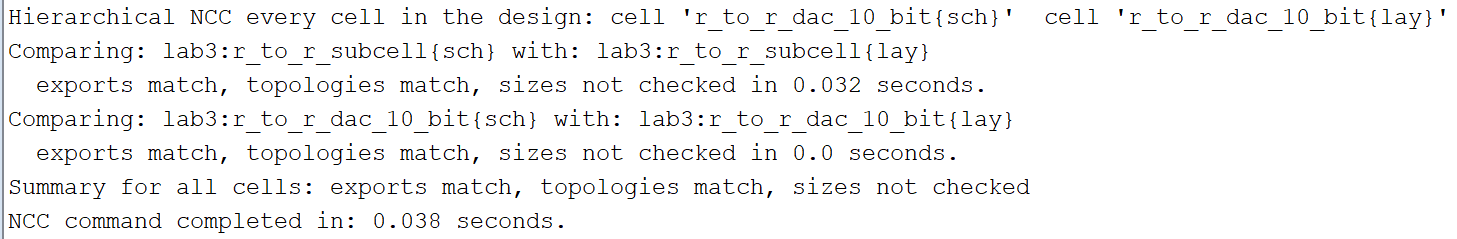
DRC, ERC and NCC where also run for the 10-bit DAC layout and also returned nothing.
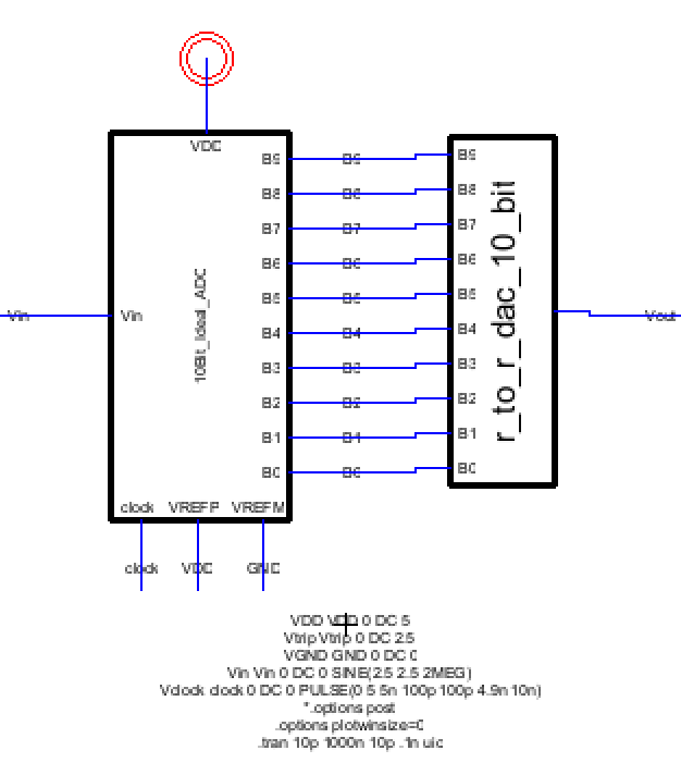
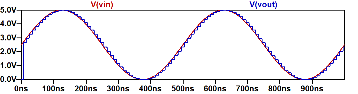
The 10-bit DAC was then connected to an ideal ADC and a AC power source to evaluate the DAC's performance. This was then simulated with LTspice.
Results
The following shows the results of the simulation.
Discussion
The simulation produced expected results, specifically in regards to how the output follows the input signal in discrete steps.