Lab 2
CE 351
James Ferguson
Introduction
The goal of this lab is gain experiance with Analog to Digital Converters (ADC) and Digital to Analog Converters (DAC) by simulating both in Electric VLSI and LTspice as well as creating a schematic for a R to R DAC.
Methods
This lab was broken up into three tasks.
Task 1
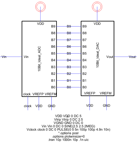
Lab matterials where downloaded. The Electric VLSI libraries included a ADC and DAC which where simulated with LTspice.
Task 2
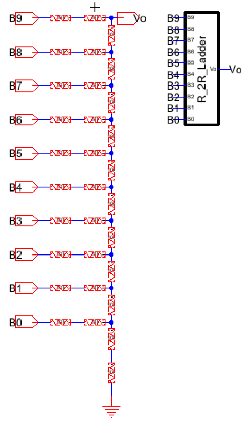
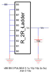
A 10-bit R to R ladded schematic was designed as instructed using 10KΩ resistors. The Following shows the resulting schematic.
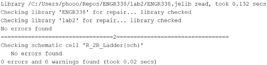
This R to R ladder DAC was then used to replace the downloaded DAC and a new simulation was ran.
DRC was run and returned in no errors.
Task 3
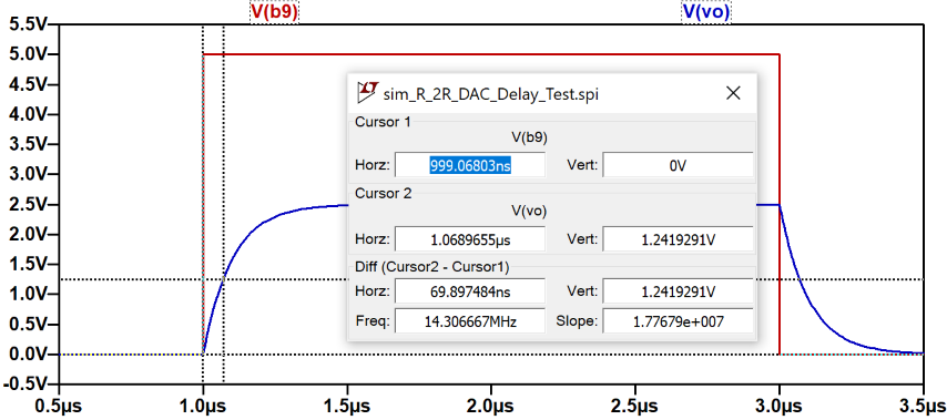
The timedelay was then sumulated for this R to R DAC with a 10pF load.
Results
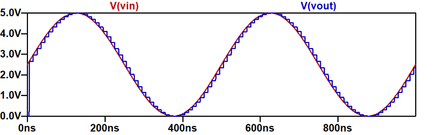
The following graph shows simulated voltages for task 1.
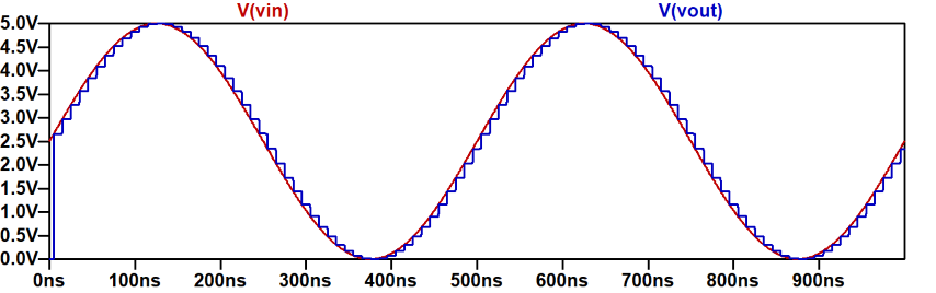
The following graph shows simulated voltages for task 2.
The following graph shows simulated voltages for task 3.
Discussion
The task 1 simulation produced expexted results as well as the task 2 simulation. The timedelay for the simulated R to R ladder DAC was shown to have a time delay of 0.07µs. this could be inproved by reducing the resistance of the R to R ladder