CE338 Digital VLSI Design 2023 Fall
Course Project SAR_ADC Full Circuit
Name: Jesse Moder
Email:
jmmoder@fortlewis.edu
1. Title
Course Project SAR_ADC Full Circuit
2. Introduction
A successive-approximation-register analog-to-digital converter (SAR ADC) is a low-power, low-footprint ADC useful for small, portable devices.
The SAR ADC works by comparing the digital ouput to the input analog
signal with successive aprroximations until the final digital output is
released
by the clock circuit. The clock circuit passes the signal to the second
R2R ladder ADC after the 10th cycle of the clock, and resets the ADC on
the 11th
cycle.
3. Materials and Methods
The circuits for the 8-bit R2R ladder DAC, the door register, and the
clock were constructed using electric VLSI. The sample and hold circuit
was connected to the SAR block.
The 8 outputs from the SAR were connected to the R2R ladder DAC. The
wires between the SAR and DAC were connected to the inputs for the door
register. The 8 outputs
from the door register were connected to the second ladder DAC. The
output from the first ladder DAC was connected to the vm port of the
comparator. The output voltage
was measured at the Vout output of the second ladder DAC.
4. Results
Figure 1 shows the 8-bit R2R ladder DAC and the DRC.
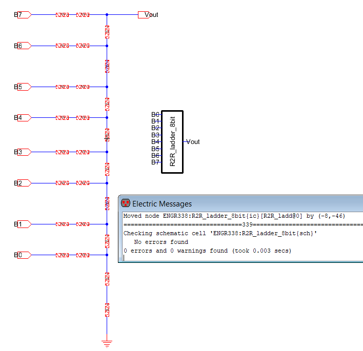
Figure 1: 8-bit R2R ladder DAC and the DRC.
Figure 2 shows the schematic of the door register and the DRC.
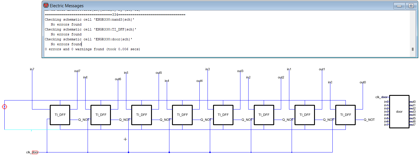
Figure 2: Schematic of the door register.
Figure 3 shows the
clock circuit constructed from 5 DFF's, as well as the circuits for
clk_door, clk_reset, SAR_SR, clk_SH, and the DRC.
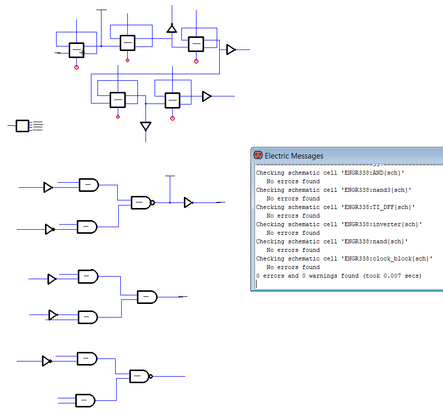
Figure 3: Clock
circuit schematics.
Figure 4 shows the full circuit for the SAR_ADC and the DRC.
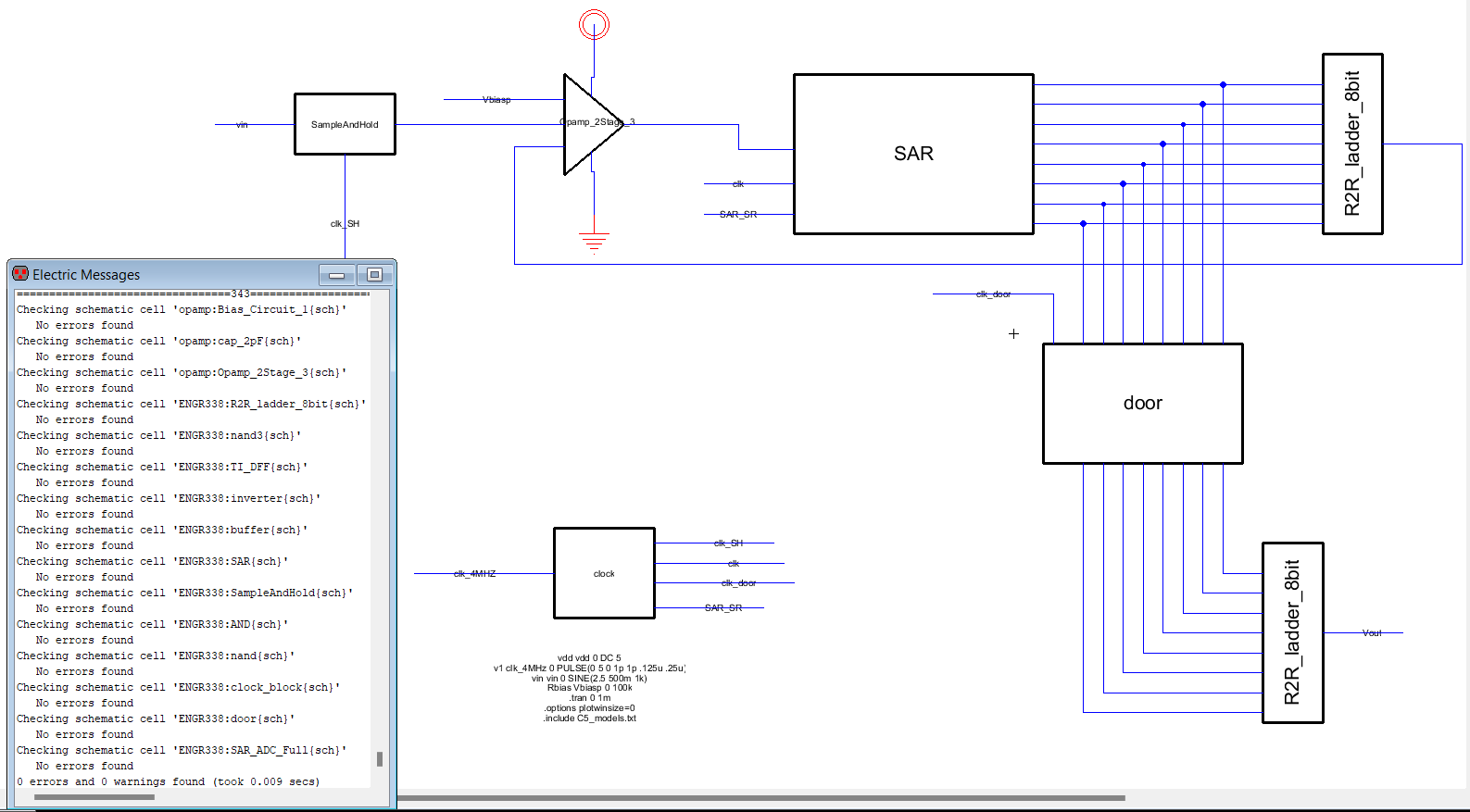
Figure 4: SAR_ADC full circuit.
Figure 5 shows the LTSpice simulation of the SAR_ADC schematic.
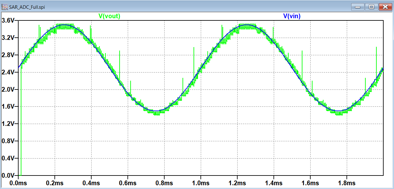
Figure 5: LTSpice simulation of the SAR_ADC schematic.
5. Discussion
Besides the time it took to construct each circuit, the clock circuit
was the most challenging aspect of the full SAR_ADC circuit. There was
a dangling arc in this circuit
that was affecting the output of each of the three subcircuits of the
clock circuit. I thought I had cleared any DRC errors, but there was
still the one error.
After fixing the dangling arc, the circuit simulated correctly. The
circuit did not hold the sample as well as I expected, as the output
signal sometimes dropped near the
original signal before sampling. A faster clock may help to fix this issue, but the output signal generally tracked the input signal well.
Question 7:
a) It is difficult to compare the time steps with the two simulations,
since the time range is unclear for the first simulation. The amplitude
of the sine wave for the
first simulation is greater than the amplitude of the second
simulation. The resolution will be the same if both ADC's have the same
number of bits. The clock
speed for the second simulation appears to be greater than the first.
b) There is a signal delay at the beginning of the simulation because
the signal needs time to move through the circuit before it can begin
outputting a voltage.
There is a time delay through the CMOS components of the circuit.
c) Comparing Vout to Vin is useful to confirm the logic of the circuit.
Comparing the node out of the sample and hold circuit to the input is
the same analog
signal. Some applications require an anolog signal converterd to a digital signal, like music files, cell phone signals, and imaging.
Question 8:
LSB = Vref/2^n = 5V/2^8 = 19.5 mV ....