CE338 Digital VLSI Design Lab 2023 Fall
Lab 9 8-bit ALU
Name: Jesse Moder
Email:
jmmoder@fortlewis.edu
1. 8-bit ALU
2. Introduction
The objecctive of this lab was to build and 8-bit ALU using Electric VLSI.
3. Materials and Methods
Electric VLSI was used to design an 8-bit ALU. The schematic of the
ALU was created using an 8-bit AND, an 8-bit OR, a high-speed full
adder, three 8-bit MUX, an 8-bit inverter,
and three regular inverters. The 8-bit inverter was created for the ALU
and the other components were created in previous tutorials. The
schematic of the ALU was simulated using
LTSpice to test the logic of the AND, OR, Add, and Subtract functions.
The layout of the ALU was created and passed the DRC and NCC.
4. Results
Figure 1 shows the layout of the 8-bit inverter, DRC and NCC.
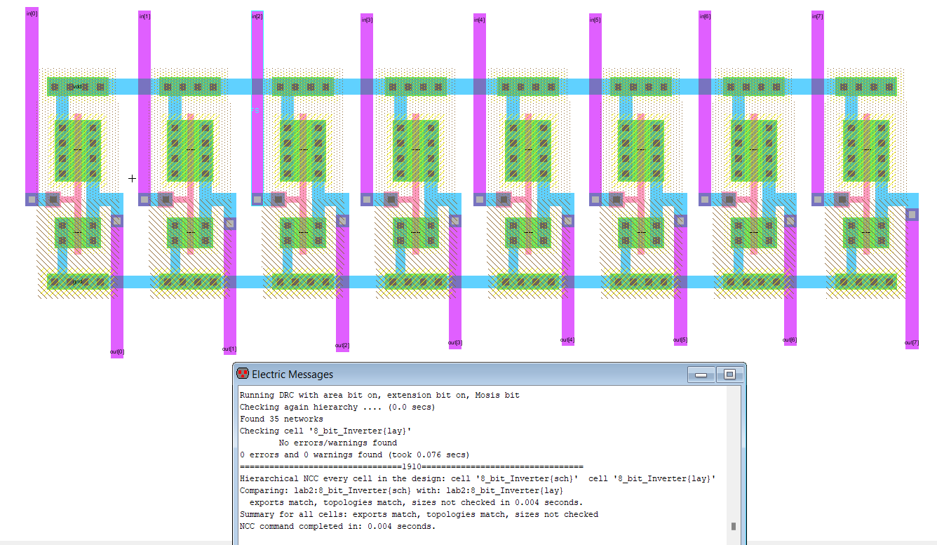
Figure 1: The layout of the 8-bit inverter, DRC and NCC.
Figure 2 shows the schematic of the 8-bit ALU and the NCC.
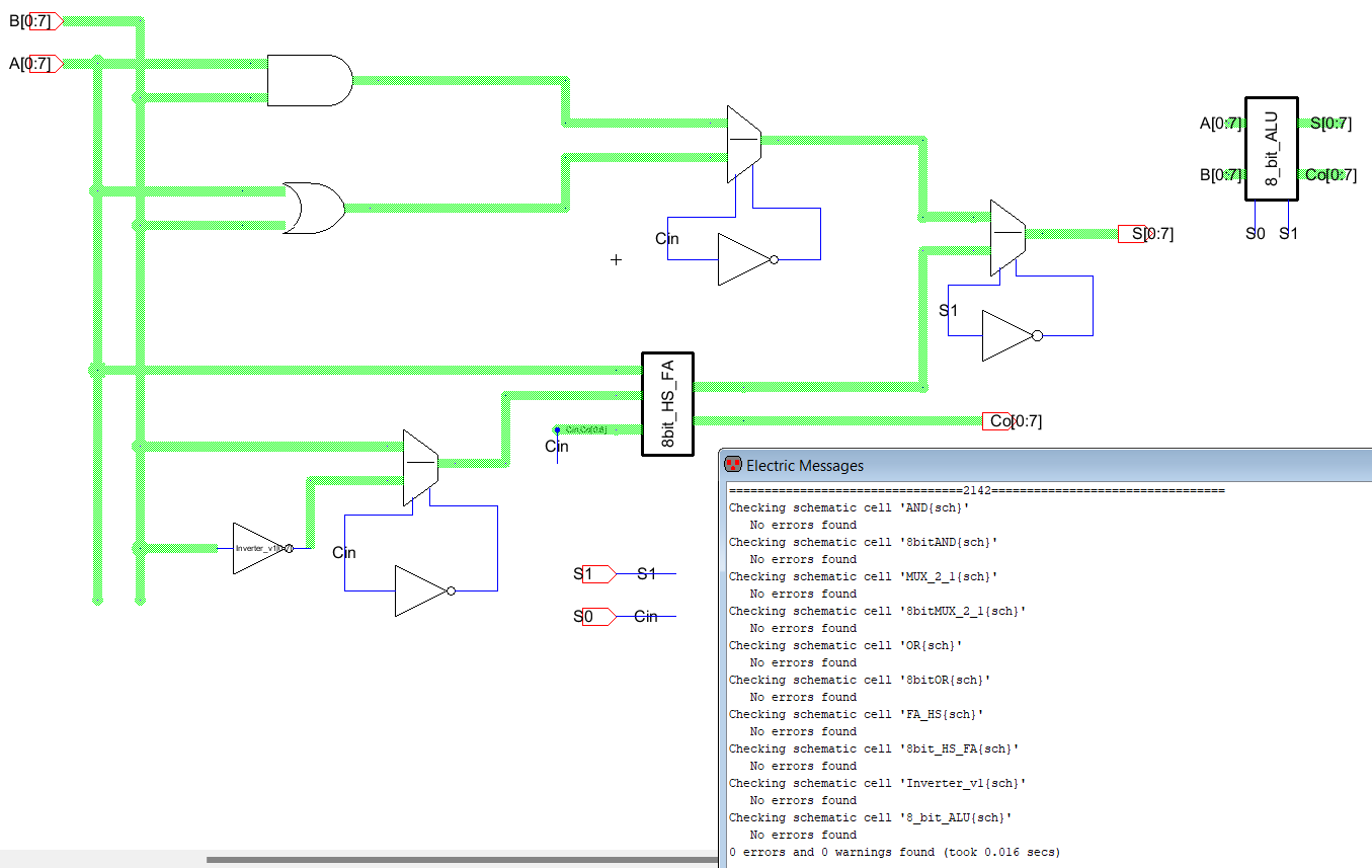
Figure 2: The schematic of the 8-bit ALU and DRC.
Figure 3 shows the simulation schematic for the AND logic, DRC, and the LTSpice simulation.
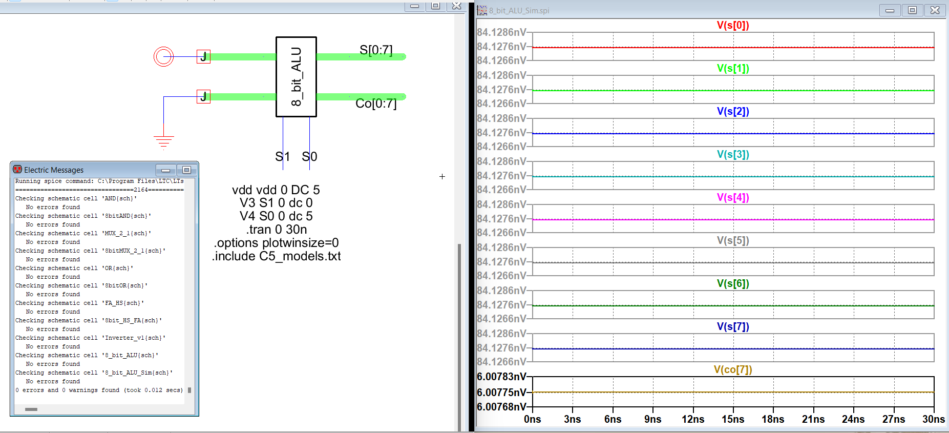
Figure 3: The simulation schematic for the ALU AND logic, DRC and LTSpice simulation.
Figure 4 shows the simulation schematic for the OR logic, DRC, and LTSpice schematic.
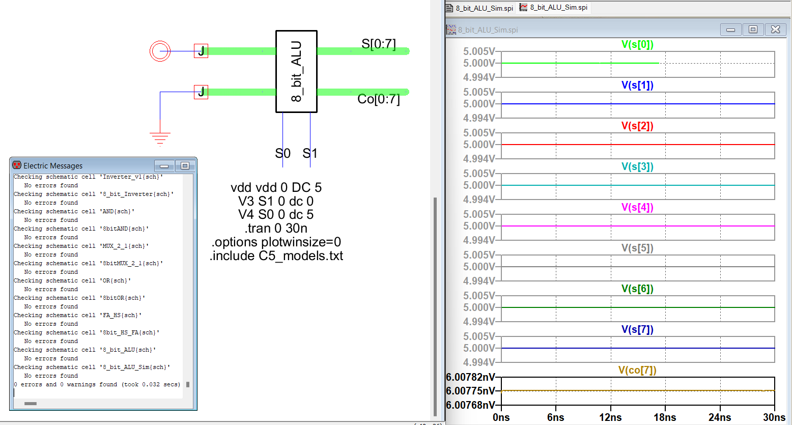
Figure 4: The simulation schematic for the ALU OR logic, DRC and LTSpice simulation.
Figure 5 shows the simulation schematic for the Add logic, DRC, and LTSpice schematic.
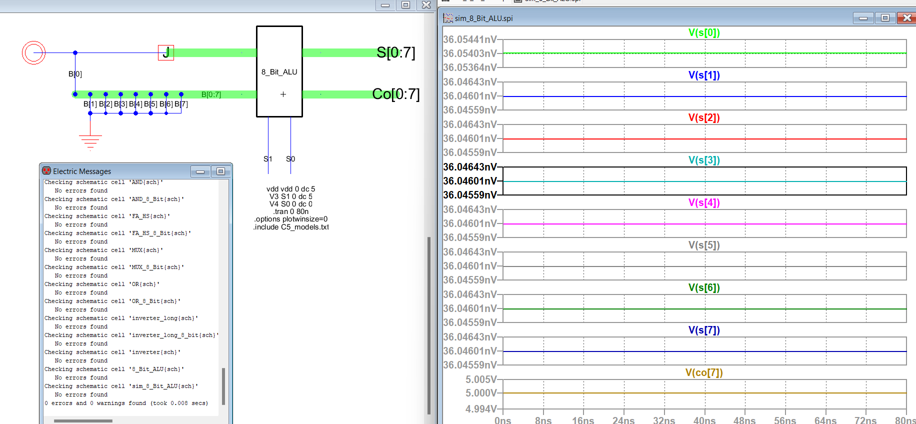
Figure 5: The simulation schematic for the ALU Add logic, DRC and LTSpice simulation.
Figure 6 shows the simulation schematic for the Subtract logic, DRC, and LTSpice schematic.
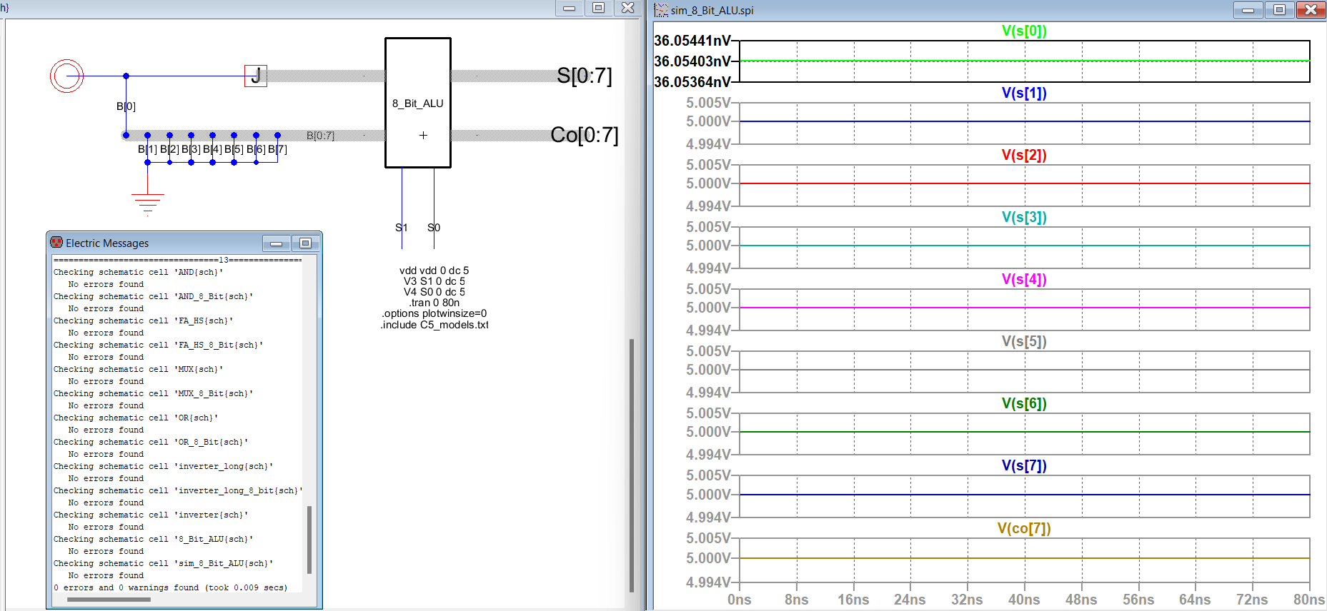
Figure 6: The simulation schematic for the ALU subtract logic, DRC and LTSpice simulation.
Figure 7 shows the layout of the 8-bit ALU, DRC, and NCC.
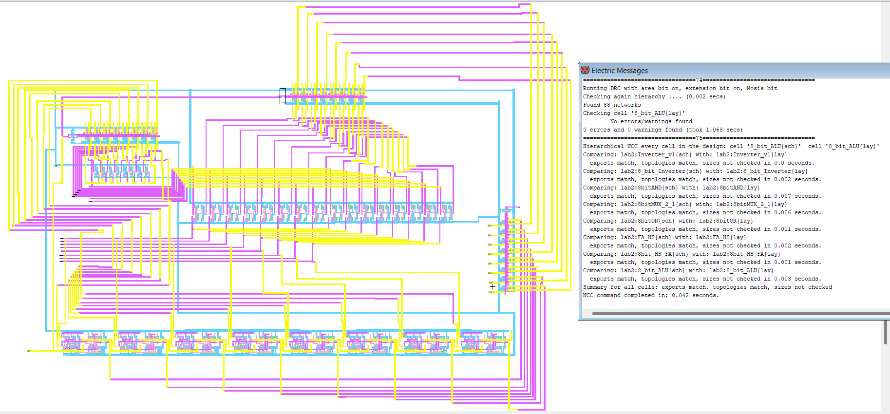
Figure 7: The layout for the 8-bit ALU, DRC, and NCC.
5. Discussion
The layout of the 8-bit ALU was especially challenging but it was
also one of the best learning experiences yet for creating a circuit
using ElectricVLSI. Resolving the NCC errors was difficult,
but experience with previous layouts helped to determine how to solve
the errors. I had the connections switched for the inputs to the MUX
from the AND and OR gates on the first try as well as
the connections from the 8-bit inverter to the MUX. The NCC errors were
confusing at first, since the wire connections were listed as missing
in either the layout or schematic, but were also present
when the wire error was clicked on. After inspecting the schematic more
closely and paying close attention to the input variable locations, I
was able to make the correct connections and eliminate the NCC errors.
Stepping through the NCC errors was very good practicefor creating more
complicated schematics and learning how to eliminate errors more
quickly in the future.