CE338 Digital VLSI Design Lab 2023 Fall
Lab 8 Design an 8-bit MUX and a High-Speed Full Adder
Name: Jesse Moder
Email:
jmmoder@fortlewis.edu
1. Design an 8-bit MUX and a High-Speed Full Adder
2. Introduction
The objectives of this lab were to build an 8-bit MUX and an 8-bit high-speed full adder using ElectricVLSI.
3. Materials and Methods
ElectricVLSI was used to design an 8-bit MUX, a high-speed full adder, and an 8-bit high-speed full adder.
CMOS components were used to create a schematic for each of the three
circuits. An icon view of the schematic was then created for
simulation.
The 8-bit circuit icons were connected to the inputs and outputs using busses for efficiency. The logic was then simulated for each circuit by
exporting the circuit to LTSpice. The layout of the circuit was then created. A DRC was performed for each circuit and simulation schematic,
and a DRC and an NCC were performed for each layout.
4. Results
Figure 1 shows the 2 to 1 MUX schematic created using ElectricVLSI and the DRC.
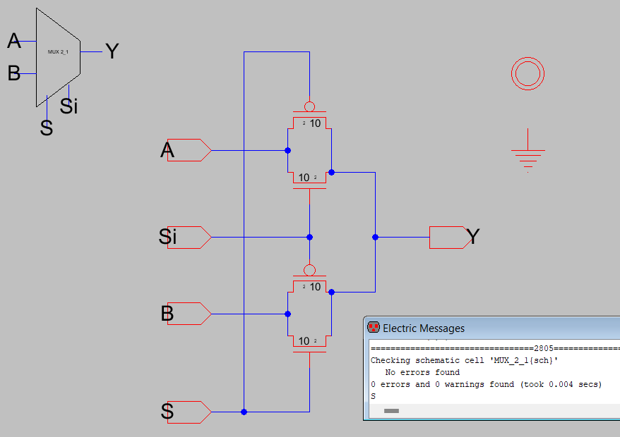
Figure 1: 2 to 1 MUX schematic.
Figure 2 shows the 2 to 1 MUX simulation schematic, the DRC, and the LTSpice simulation of VA, VB, VS, and VY.
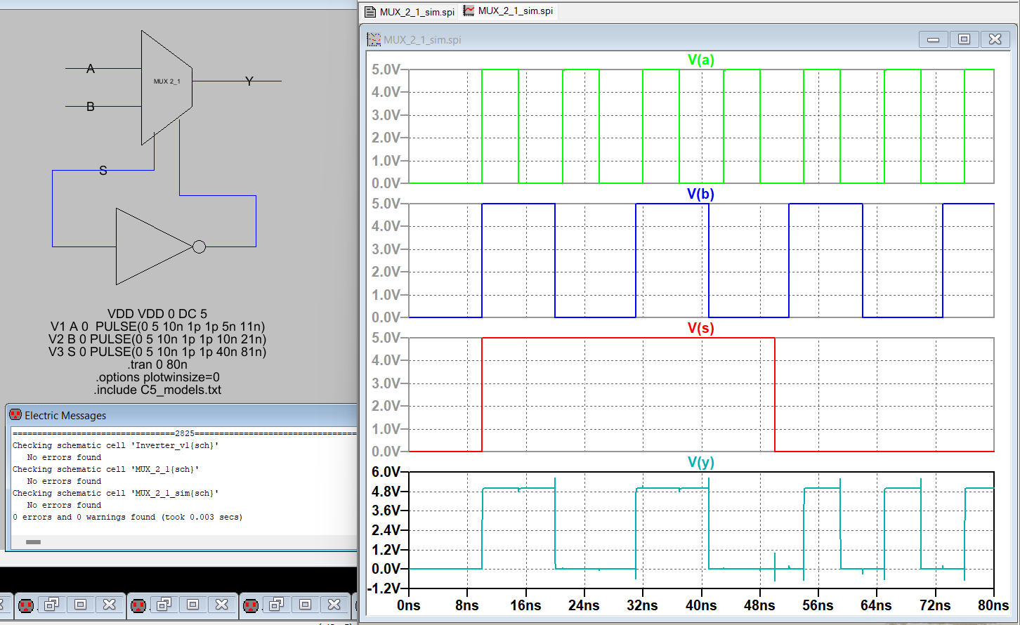
Figure 2: 2 to 1 MUX simulation schematic and simulation results.
Figure 3 shows the schematic for the 8-bit 2 to 1 MUX connected using buses and the DRC.
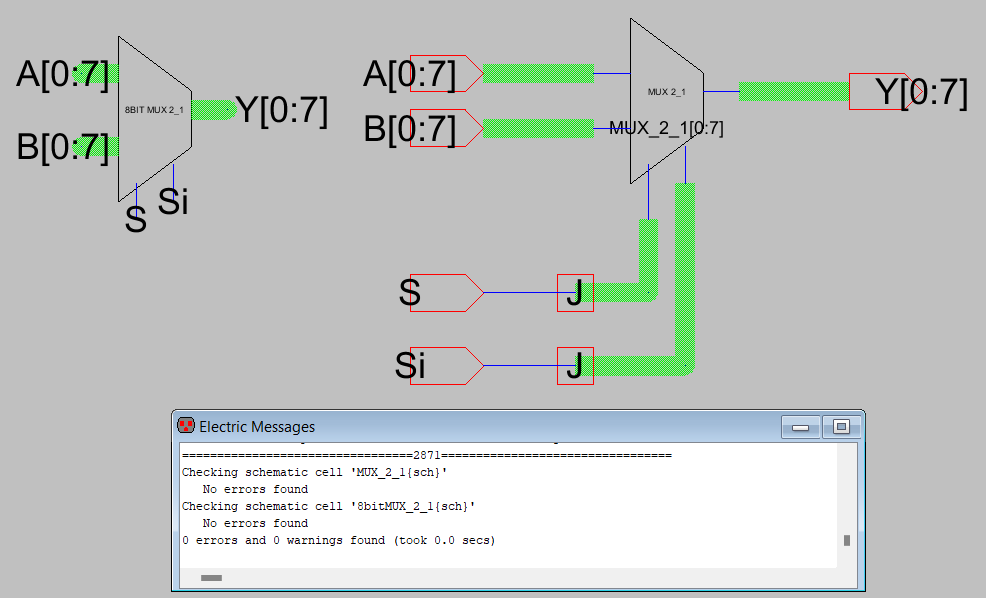
Figure 3: 8-bit 2 to 1 MUX schematic.
Figure 4 shows the 8-bit 2 to 1 MUX simulation schematic, the DRC, and the LTSpice simulation of VA, VB, VS, and VY[0:7].
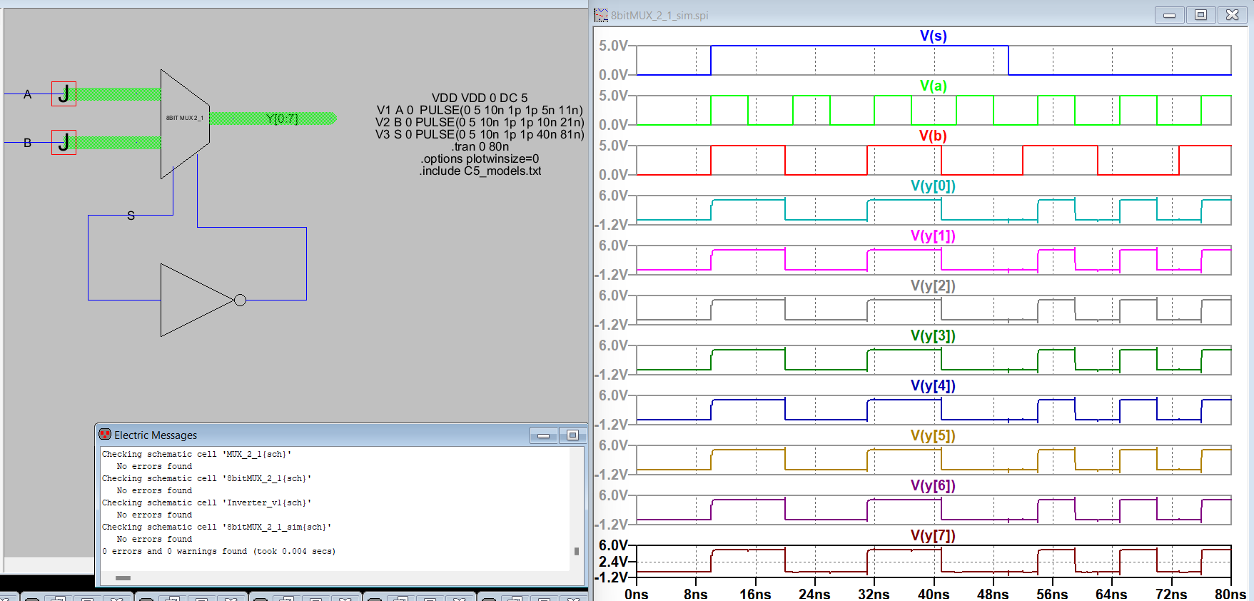
Figure 4: 8-bit 2 to 1 MUX simulation schematic and simulation results.
Figure 5 shows the layout of the 2 to 1 mux, the DRC, and the NCC.
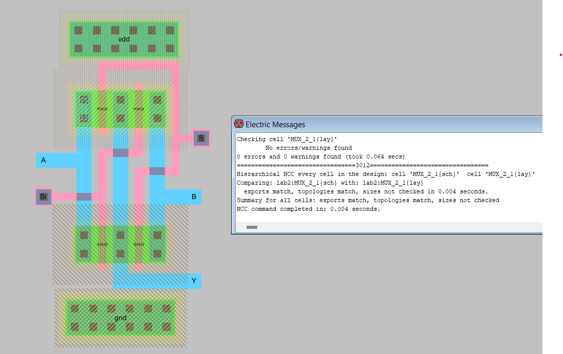
Figure 5: 2 to 1 mux layout.
Figure 6 shows the layout of the 8-bit 2 to 1 mux, the DRC, and the NCC.
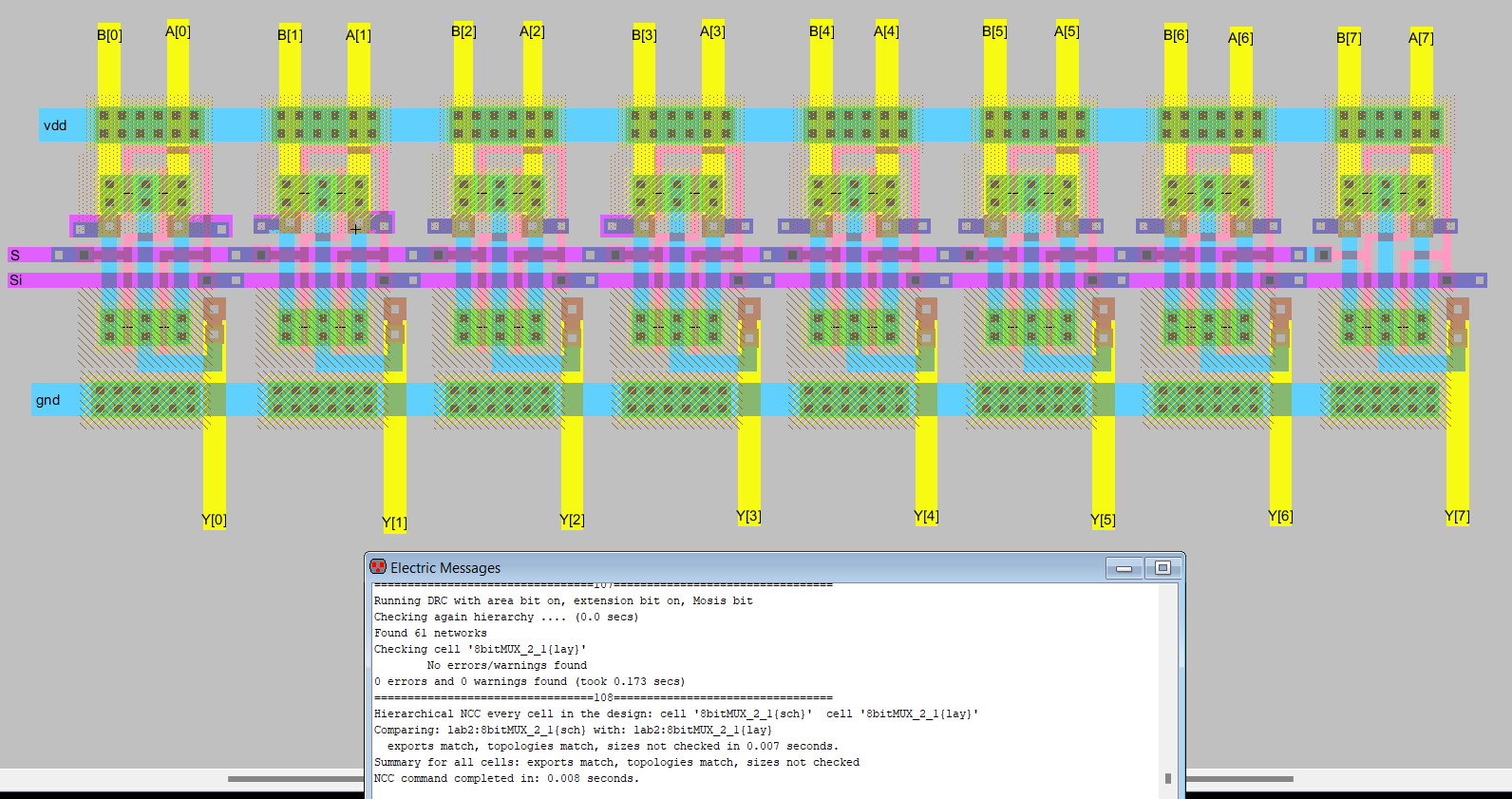
Figure 6: 8-bit 2 to 1 MUX layout.
Figure 7 shows the schematic and DRC for the high-speed full adder.
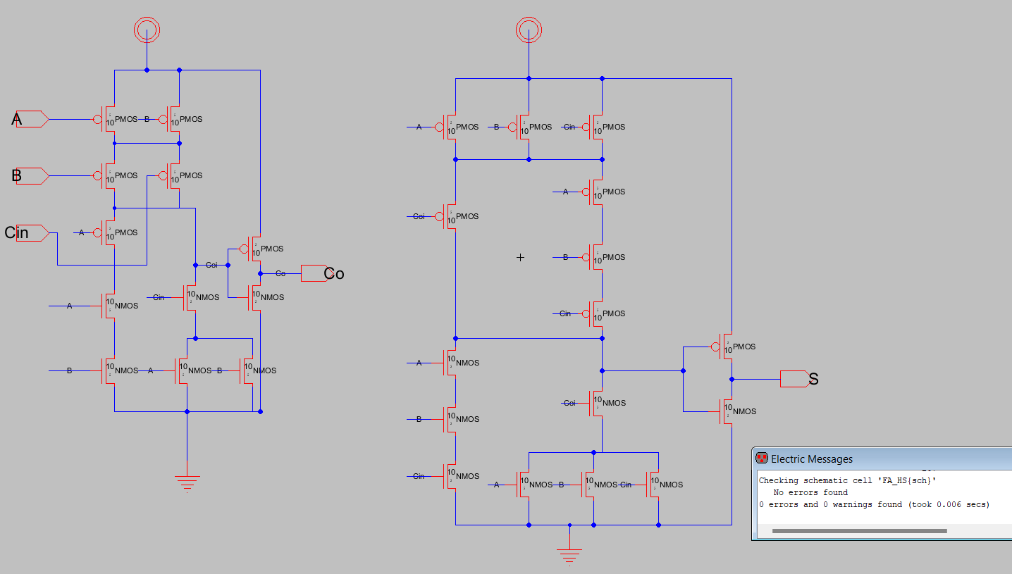
Figure 7: Schematic of the high-speed full adder.
Figure 8 shows the high-speed full adder simulation schematic, DRC, and LTSpice simulation of vA, vB, VDD, VS and VCo.
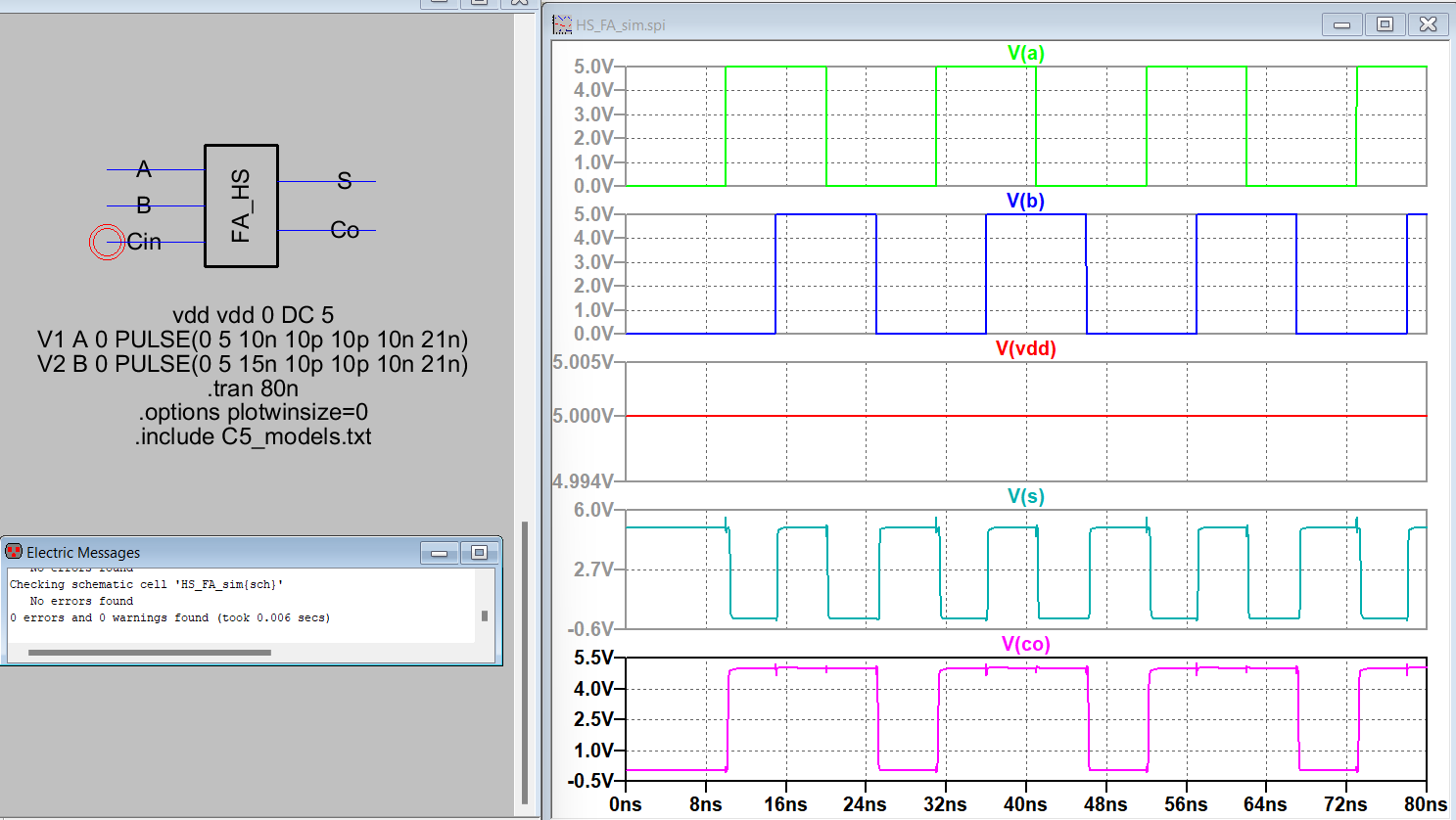
Figure 8: High-speed full adder simulation schematic and simulation results.
Figure 9 shows the layout, DRC, and NCC for the high-speed full adder.
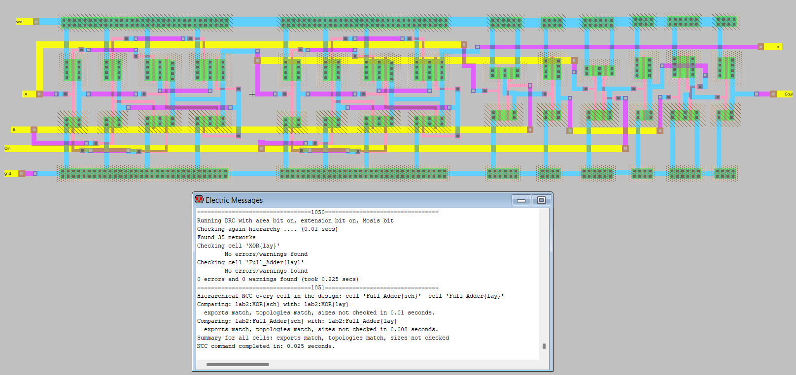
Figure 9: High-speed full adder layout.
Figure 10 shows the simulation schematic for the 8-bit high-speed full
adder, DRC, and LTSpice simulation for VS[0:7] and VCo[7].
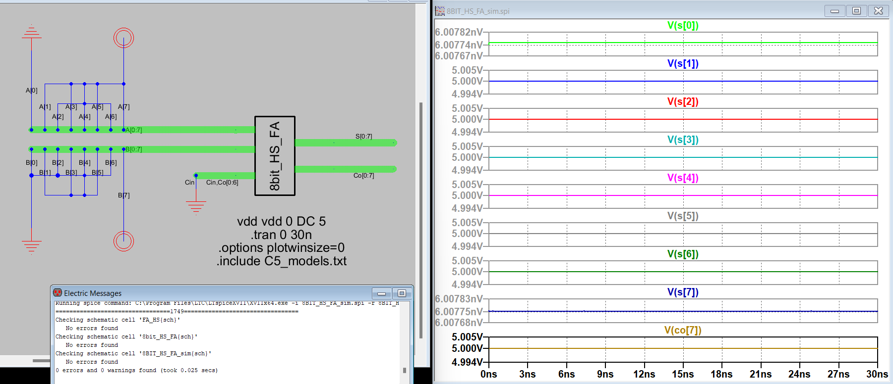
Figure 10: 8-bit high-speed full adder simulation schematic and simulation results.
Figure 11 shows the 8-bit high-speed full adder layout, DRC, and NCC.
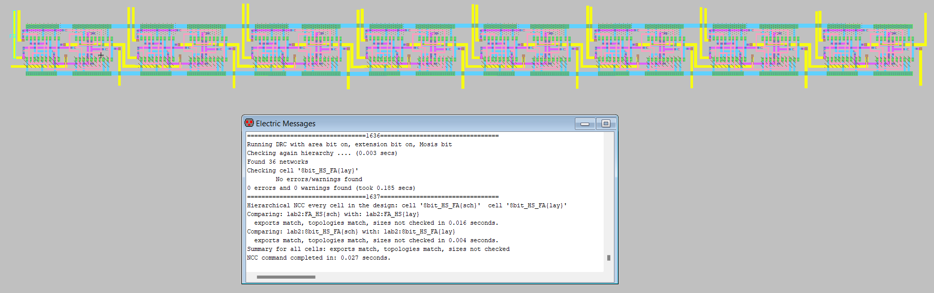
Figure 11: 8-bit high-speed full adder layout.
5. Discussion
Designing an 8-bit MUX and an 8-bit high-speed full adder was both
more challenging and less frustrating than previous ElectricVLSI
projects.
The challenges of previous projects mostly included resolving DRC and
NCC errors, as well as model file issues. For this project, it was much
easier
to avoid DRC errors with previous experience setting spice models and
learning proper spacing for the components. The challenges for this
project
included properly connecting the PMOS and NMOS components to pass the
NCC. Using buses for the schematic simulation was also challenging due
to the pins not registering as connected to the bus. After trial and
error of the order of connecting the pins to the bus, the DRC errors
resolved.
After completing this project, I feel prepared to successfully design the 8-bit ALU for the next project.