CE338 Digital VLSI Design Lab 2023 Fall
Lab 7
Name: Jesse Moder
Email:
jmmoder@fortlewis.edu
1. Using Buses in ElectricVLSI
2. Introduction
The objectives of this tutorial were to build a ring oscillator using buses and to build multi-bit gates using ElectricVLSI.
3. Materials and Methods
ElectricVLSI was used to build a ring oscillator and 8 bit AND, OR, NAND, and NOR gates. The ring
oscillator was first constructed using 11 inverters, which passed DRC and the logic was simulated.
The ring oscillator was then constructed using the inverter icon view connected to the [0:9] inputs and
[0:9] ouput with a bus and the logic was simulated. The layout icon view and ring oscillator were then
constructed.
The AND, OR, NAND, and NOR gate schematics and layouts were constructed with PMOS and NMOS components.
The OR gate was simulated to demonstrate the logic and ensure proper connections.
The 8-bit AND, OR, NAND, and NOR gate shematics with bus connections were then
constructed and simulated. The 8-bit schematics were simulated with B0, B2, B4, and B6 connected to ground and
B1, B3, B5, and B7 connected to vdd. A[0:7] were connected to vdd for simulation to demonstrate the logic.
The 8-bit layout was then constructed for each gate.
4. Results
Figure 1.1 shows the inverter short layout and DRC.
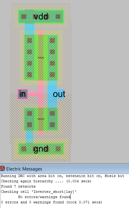
Figure 1.1: Inverter short layout.
Figure 1.2 shows the schematic of the ring oscillator, DRC, and LTSpice simulation.
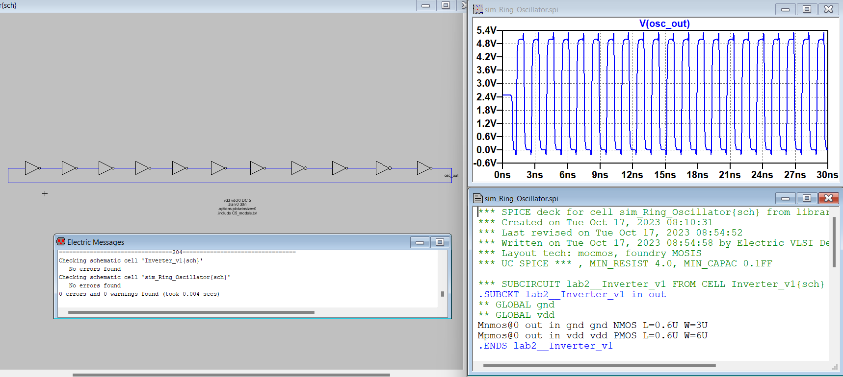
Figure 1.2: The ring oscillator and simulation.
Figure 1.3 shows the ring oscillator schematic constructed using buses, DRC, and LTSpice simulation.
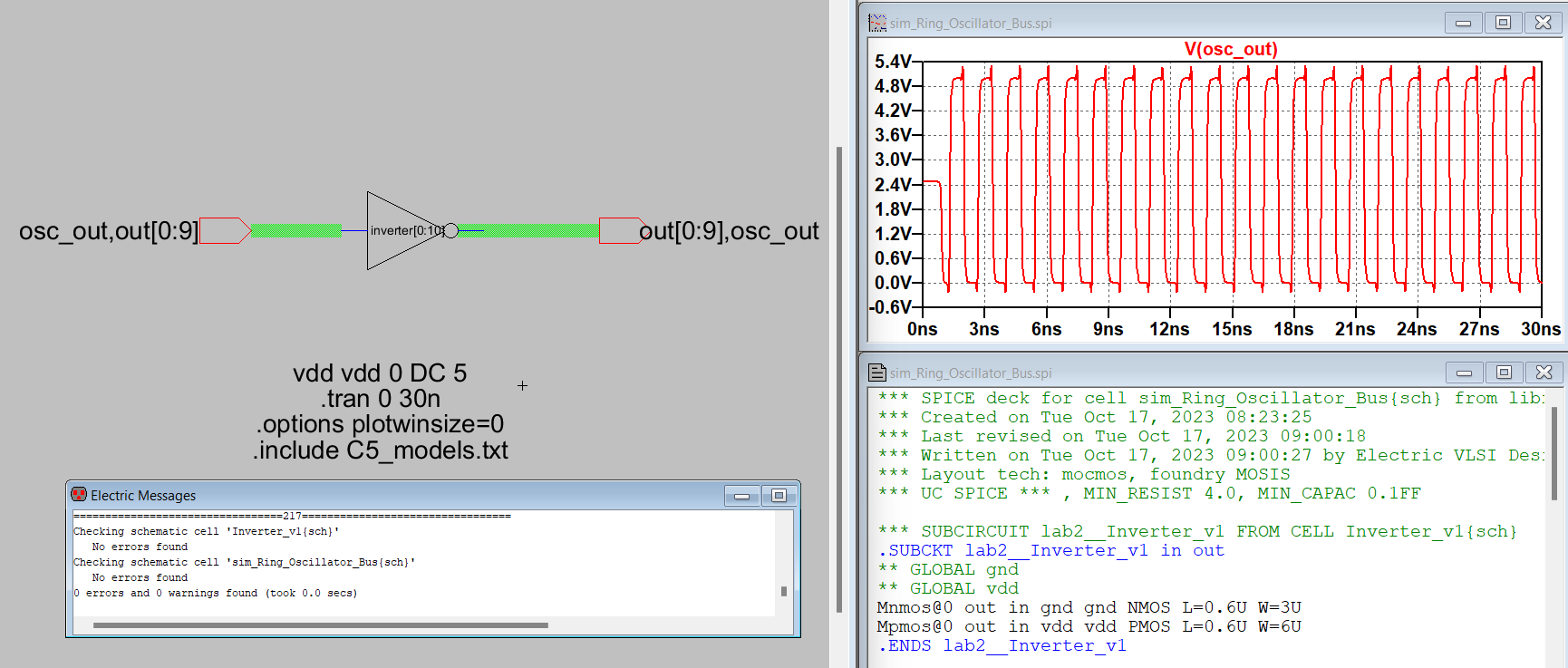
Figure 1.3: Bus ring oscillator and simulation.
Figure 1.4 shows the ring oscillator schematic using the inverter layout icons and DRC.
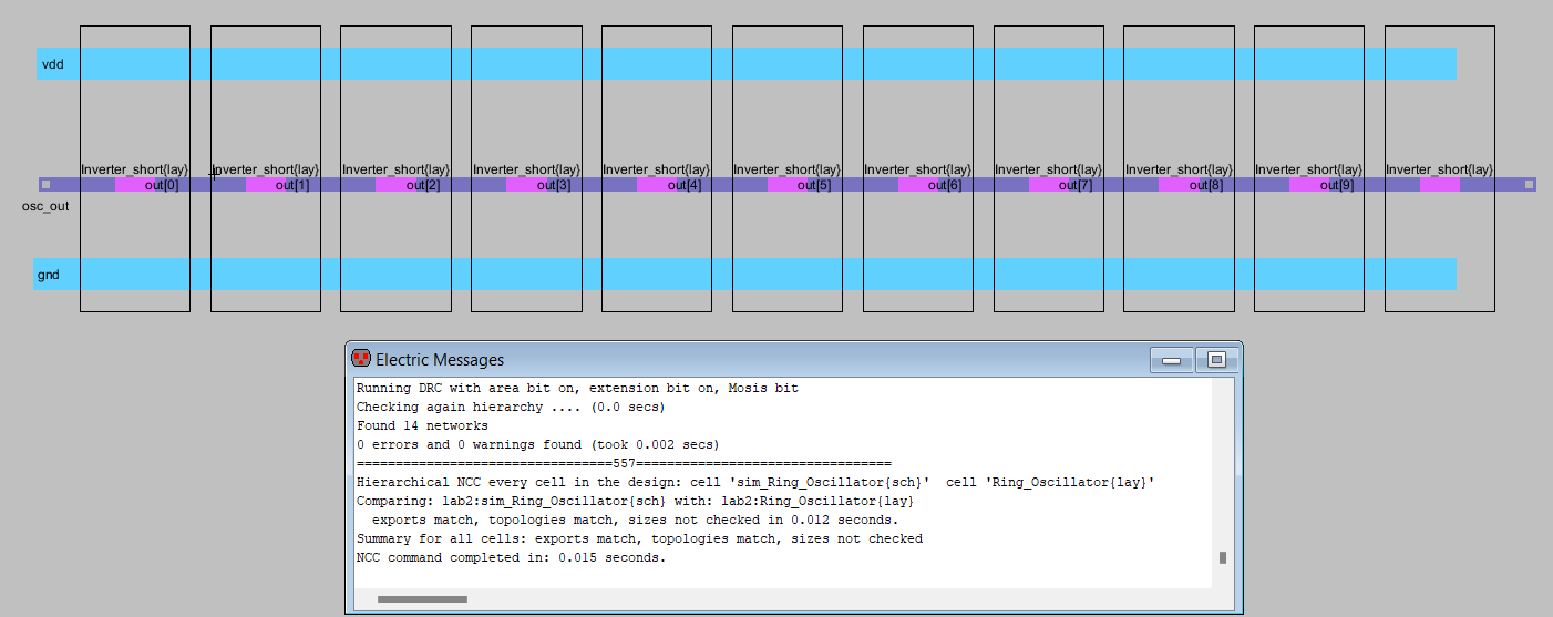
Figure 1.4: Inverter layout icon ring oscillator.
Figure 1.5 shows the ring oscillator layout and DRC.
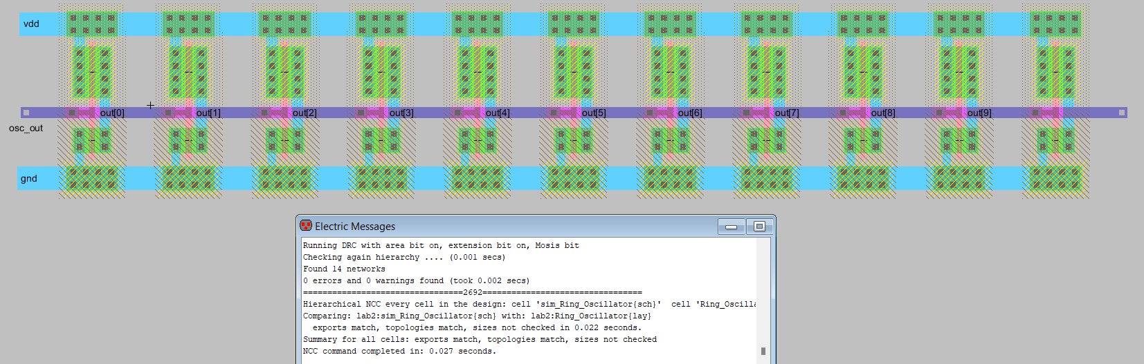
Figure 1.5: The ring oscillator layout.
Figure 2.1 shows the and gate schematic and DRC.
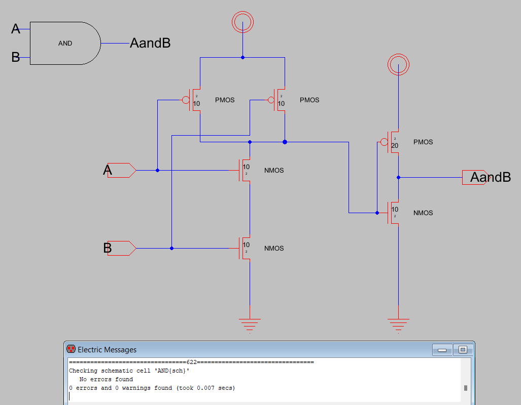
Figure 2.1: AND gate schematic.
Figure 2.2 shows the AND gate layout passing the DRC and NCC.
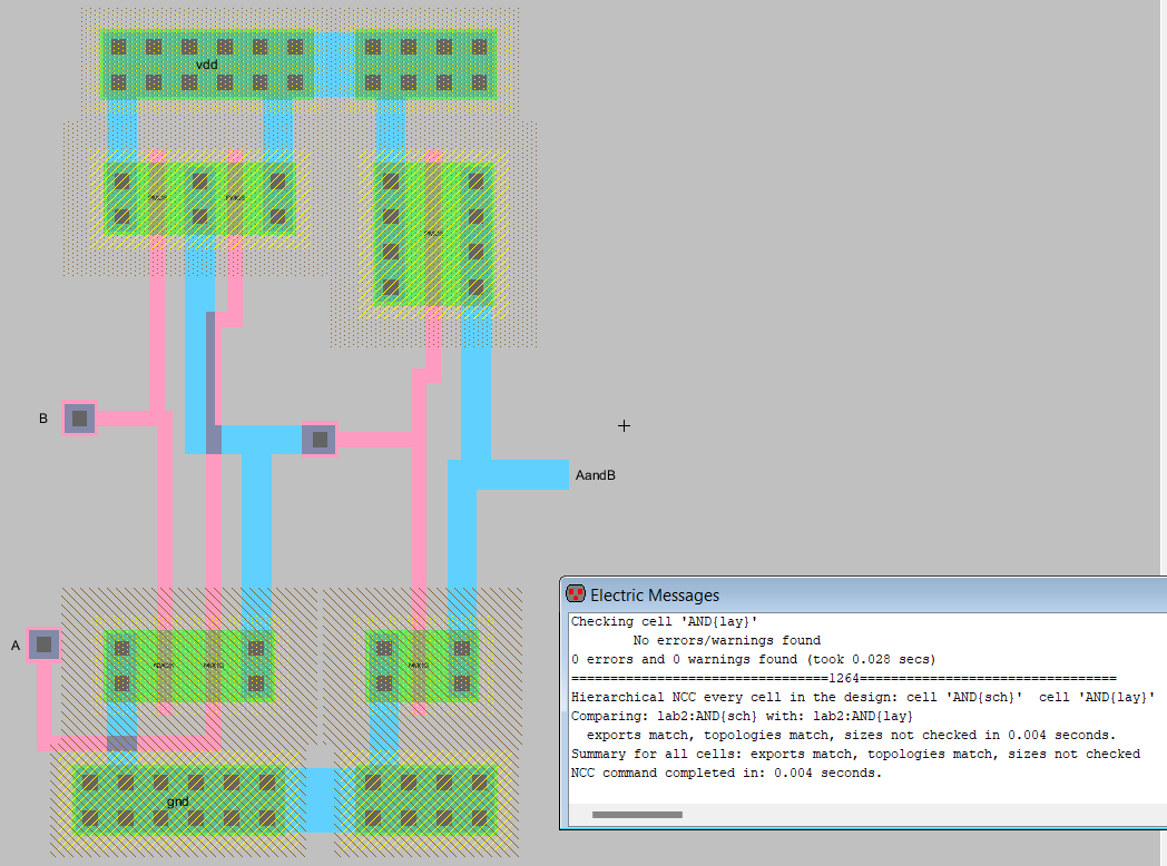
Figure 2.2: AND gate layout.
Figure 2.3 shows the 8-bit AND schematic connected using buses and DRC.
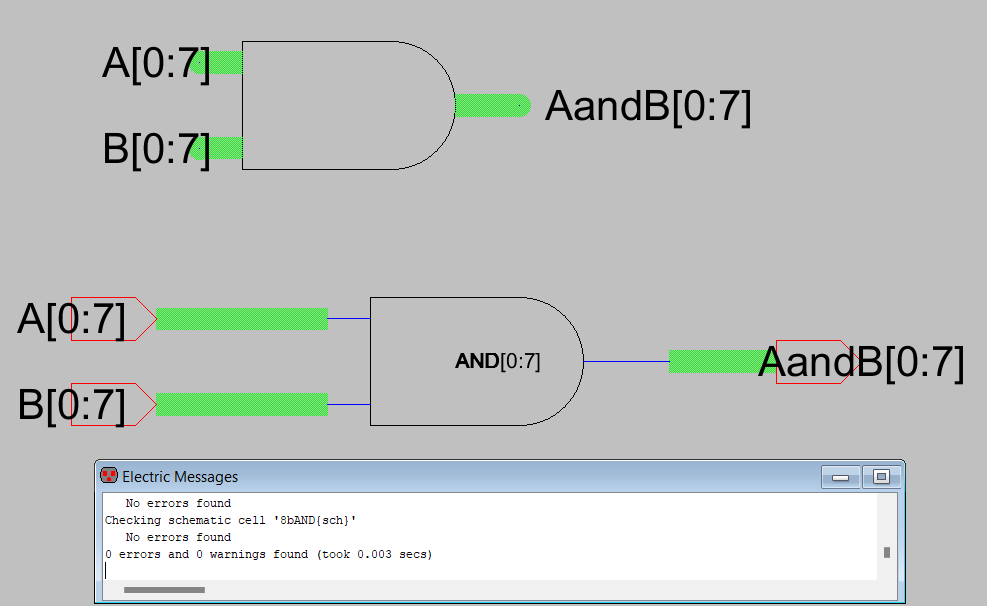
Figure 2.3: 8-bit AND gate schematic.
Figure 2.4 shows the 8-bit AND simulation schematic and LTSpice simulation with A connected to vdd.
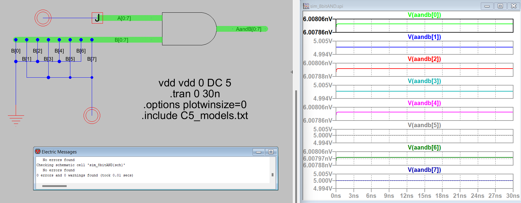
Figure 2.4: 8-bit AND simulation schematic and simulation, A connected to vdd.
Figure 2.5 shows the 8-bit AND simulation schematic and LTSpice simulation with A connected to ground.
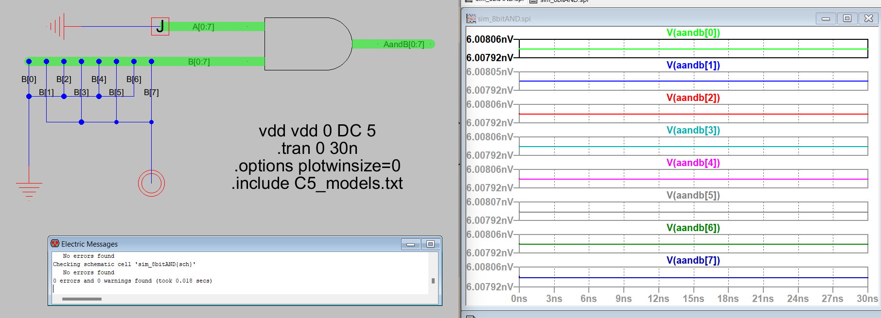
Figure 2.5: 8-bit AND simulation schematic and simulation, A connected to ground.
Figure 2.6 shows the 8-bit AND layout, DRC, and NCC check.
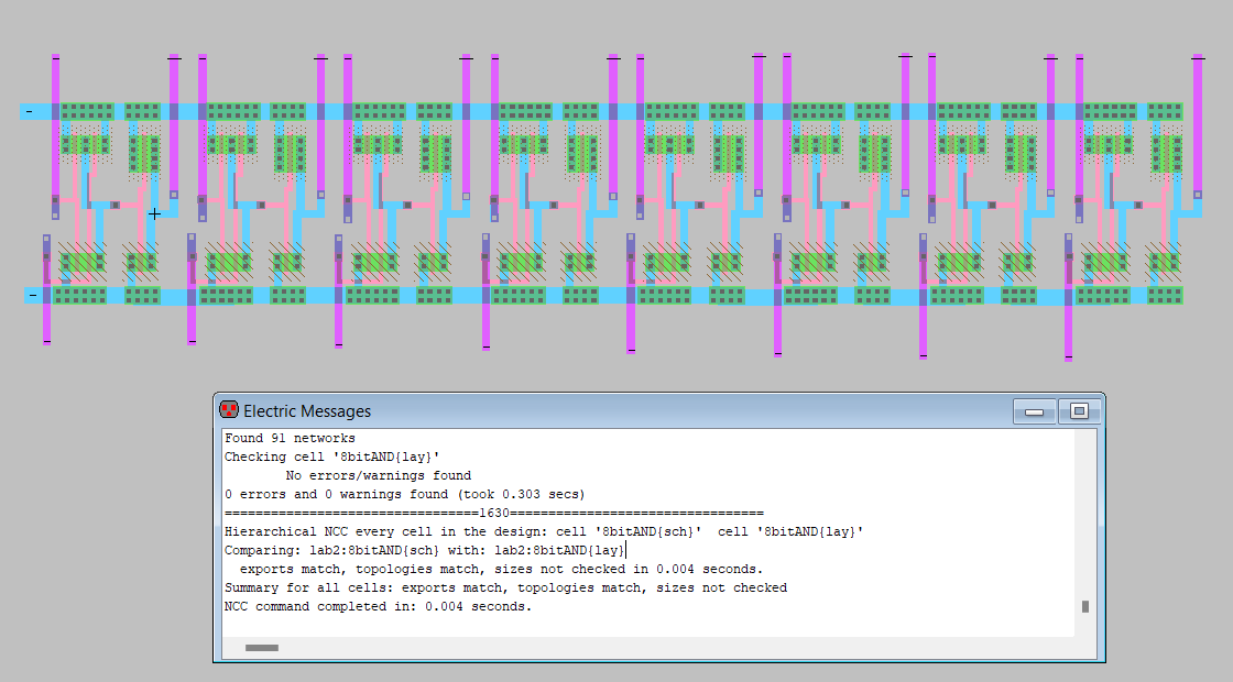
Figure 2.6: 8-bit AND layout.
Figure 3.1 shows the OR schematic and DRC.
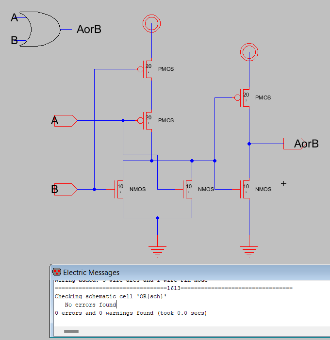
Figure 3.1: OR schematic.
Figure 3.2 shows the OR simulation schematic and LTSpice simulation.
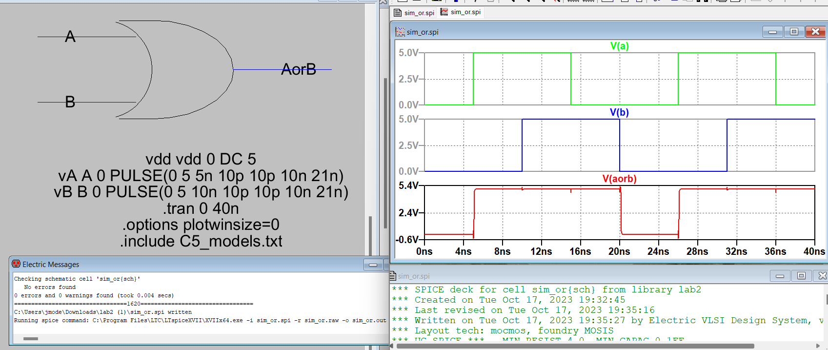
Figure 3.2: OR simulation schematic and simulation.
Figure 3.3 shows the OR layout passing the DRC and NCC.
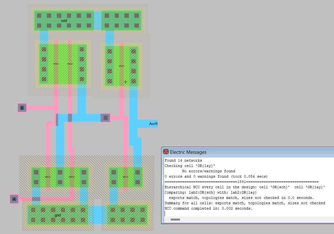
Figure 3.3: OR layout.
Figure 3.4 shows the 8-bit OR schematic and DRC.
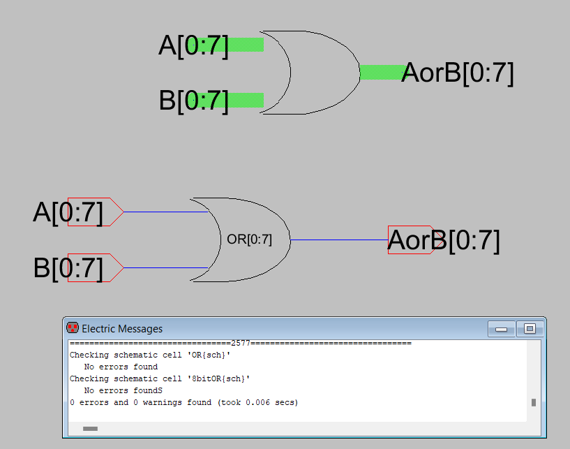
Figure 3.4: 8-bit OR schematic.
Figure 3.5 shows the simulation schematic for the 8-bit OR with A connected to vdd.
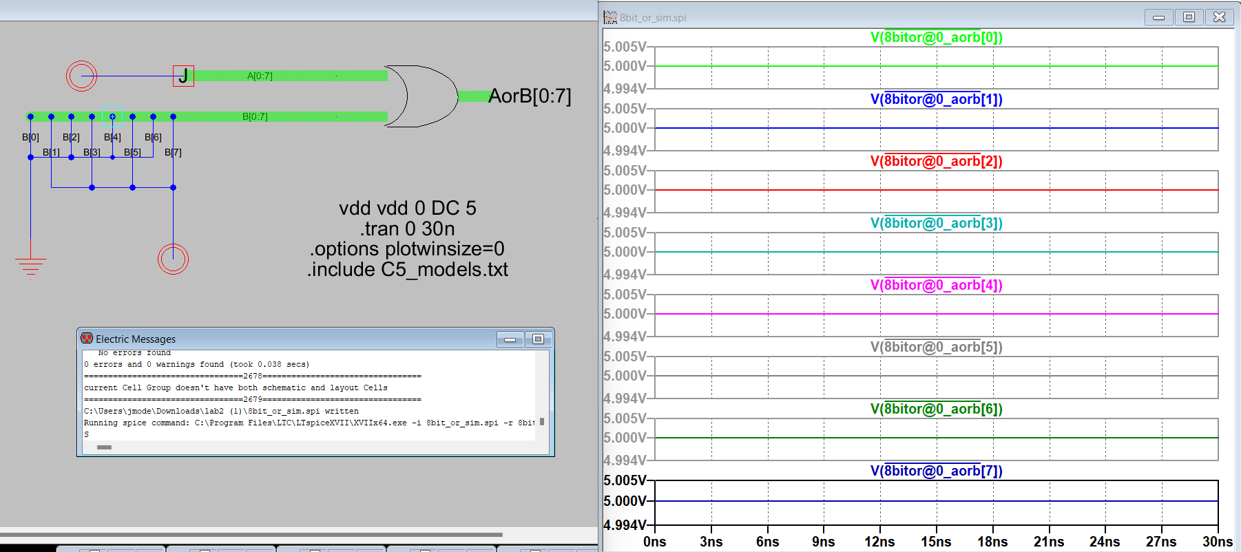
Figure 3.5: 8-bit OR simulation schematic and simulation.
Figure 3.6 shows the layout of the 8-bit OR and DRC and NCC.
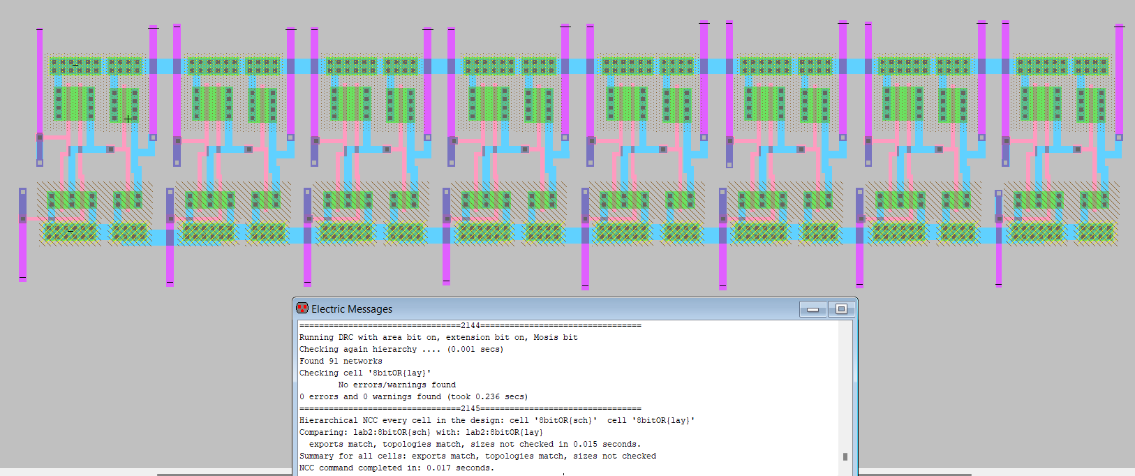
Figure 3.6: 8-bit OR layout.
Figure 4.1 shows the schematic of the 8-bit NAND and DRC.
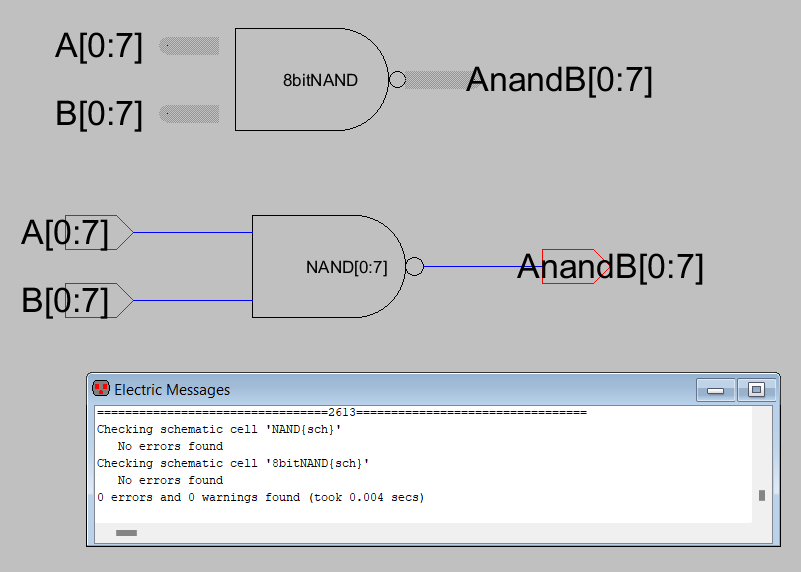
Figure 4.1: 8-bit NAND schematic.
Figure 4.2 shows the 8-bit NAND simulation schematic and LTSpcie simulation.
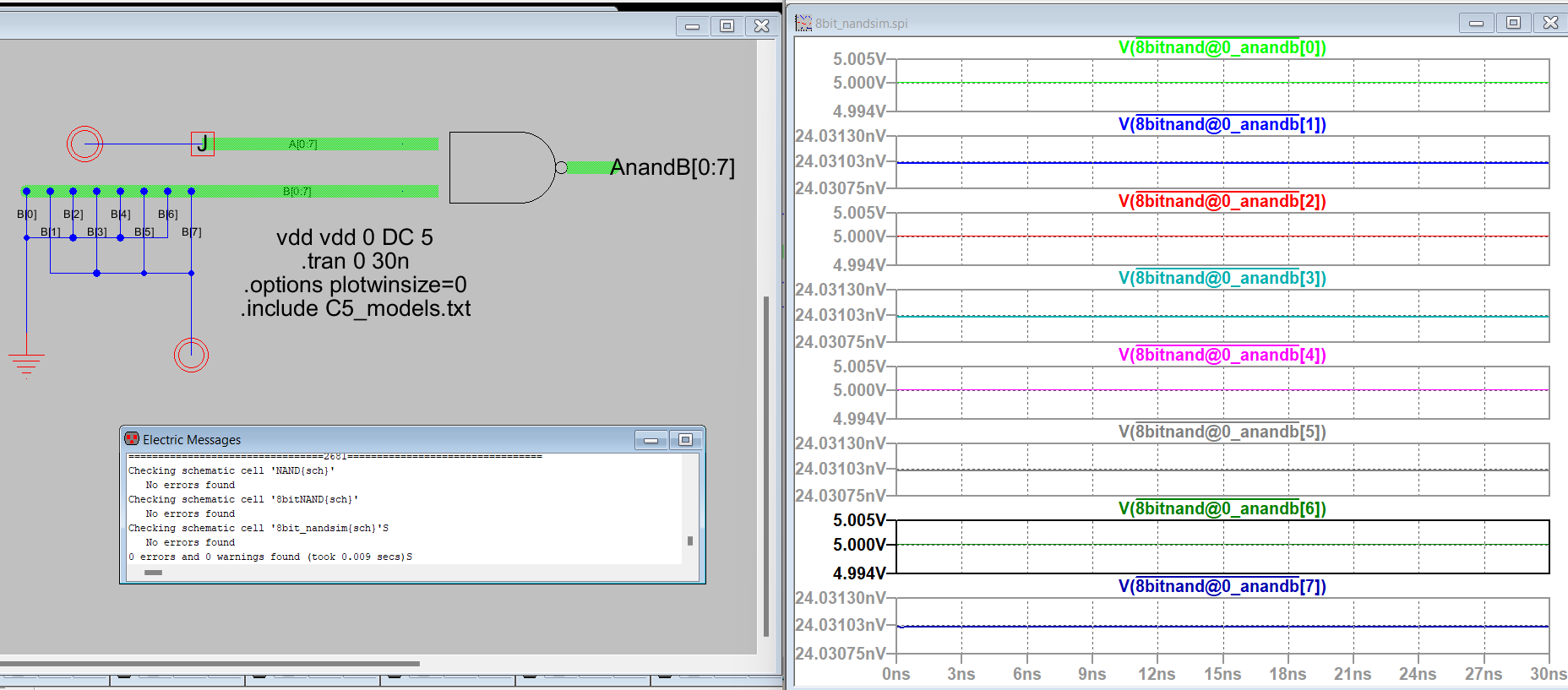
Figure 4.2: 8-bit NAND simulation schematic and simulation.
Figure 4.3 shows the 8-bit NAND layout and NCC.
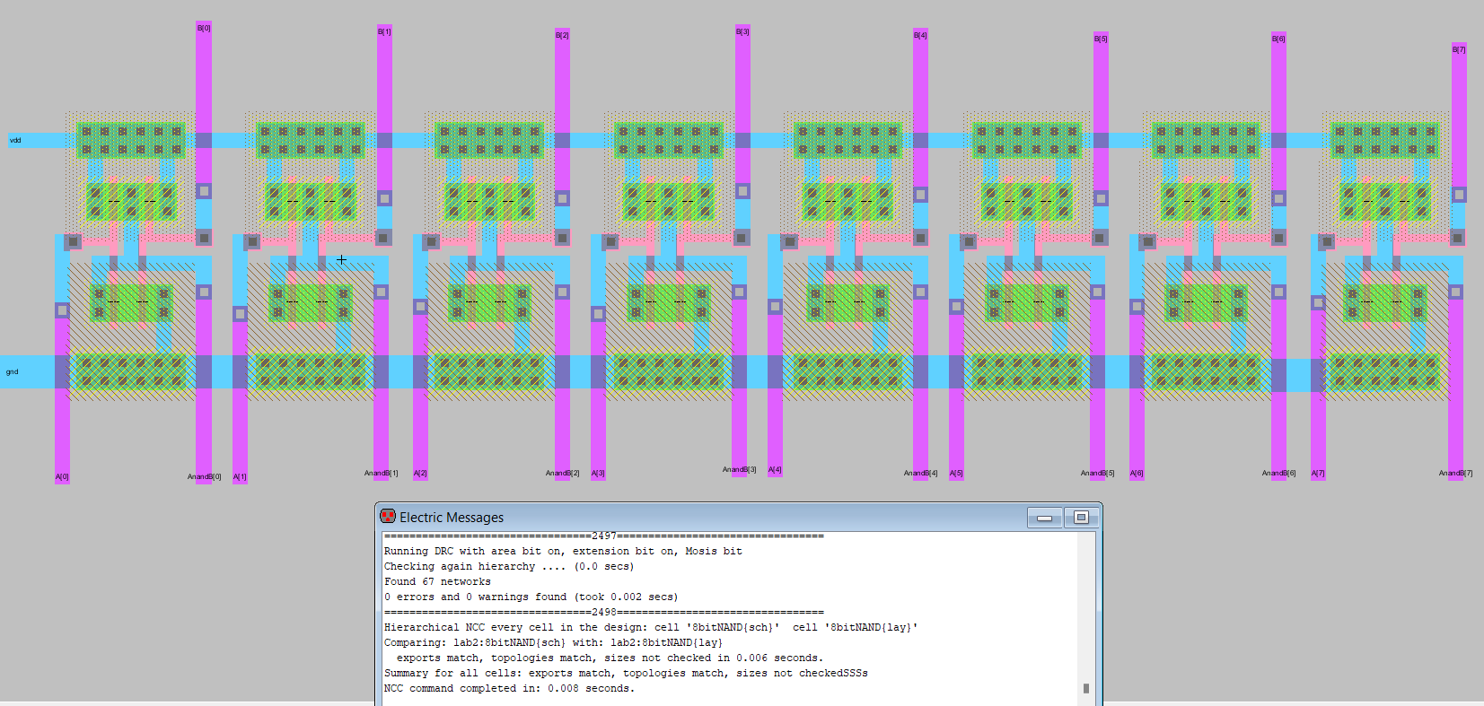
Figure 4.3: 8-bit NAND layout.
Figure 5.1 shows the 8-bit NOR schematic and DRC.
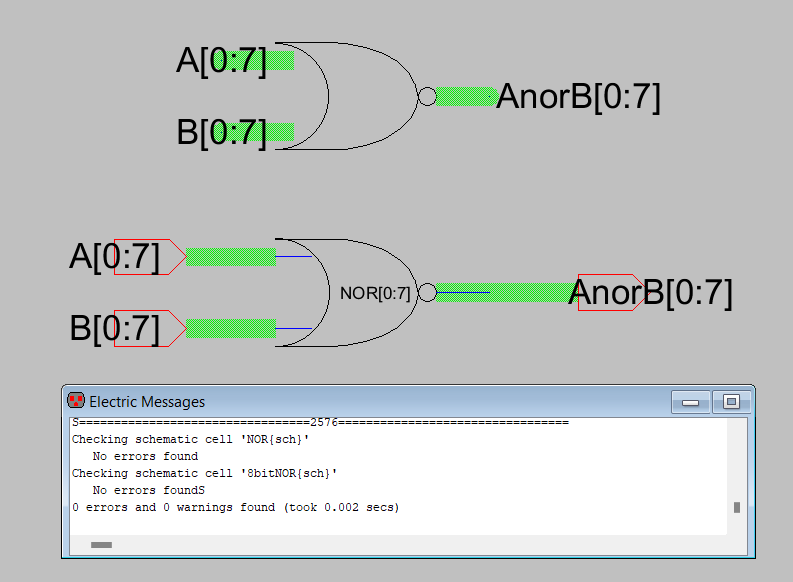
Figure 5.1: 8-bit NOR schematic.
Figure 5.2 shows the 8-bit NOR schematic and LTSpice simulation.
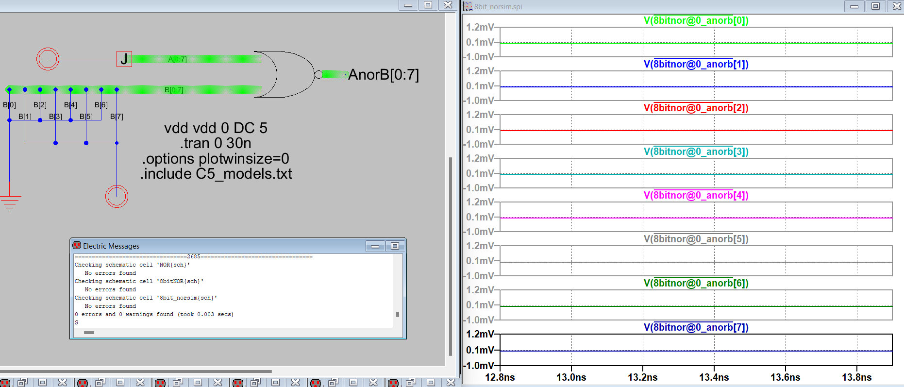
Figure 5.2: 8-bit NOR simulation schematic and simulation.
Figure 5.3 shows the 8-bit NOR layout and NCC.
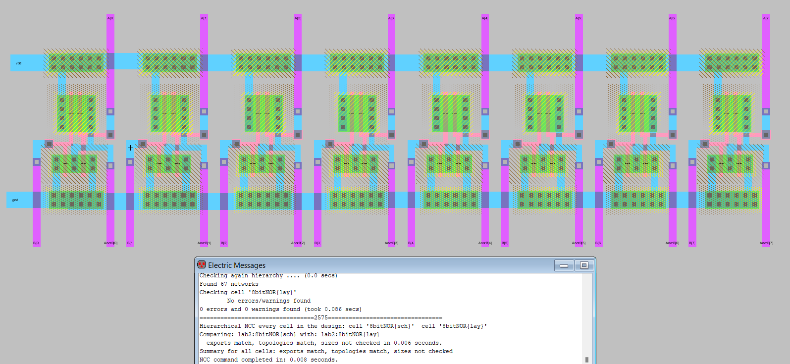
Figure 5.3: 8-bit NOR layout.
5. Discussion
Laying out mulit-bit gates was good practice for learning design
rules and ensuring all of the exports and connections match between the
schematic and layout.
Constructing the ring oscillator demonstrated how using buses is more
efficient than manually laying out the number of components required.
Practicing connecting 8-bit gates is good preperationfor the more complicated MUX and high-speed full adder layouts.