CE338 Digital VLSI Design Lab 2023 Fall
Lab 6
Name: Jesse Moder
Email:
jmmoder@fortlewis.edu
1. Build a NAND, NOR, XOR, and Full Adder
2. Introduction
The objective of this lab was to build a NAND, NOR, XOR, and Full Adder in ElectricVLSI.
3. Materials and Methods
ElectricVLSI was used to create CMOS NAND, NOR, and XOR gates, as well
as a Full Adder. The schematic, icon, and layout for each gate or
circuit
was constructed and each passed the design rule or network consistency
check. The simulation of the NAND, NOR, and XOR gates were exported to
LTSpice.
4. Results
Figure 1 shows the schematic and icon view of the CMOS NAND gate created using Electric VLSI.
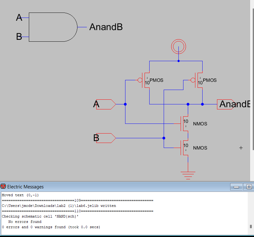
Figure 1: The schematic and icon view of the CMOS NAND gate.
Figure 2 shows the NAND gate layout.
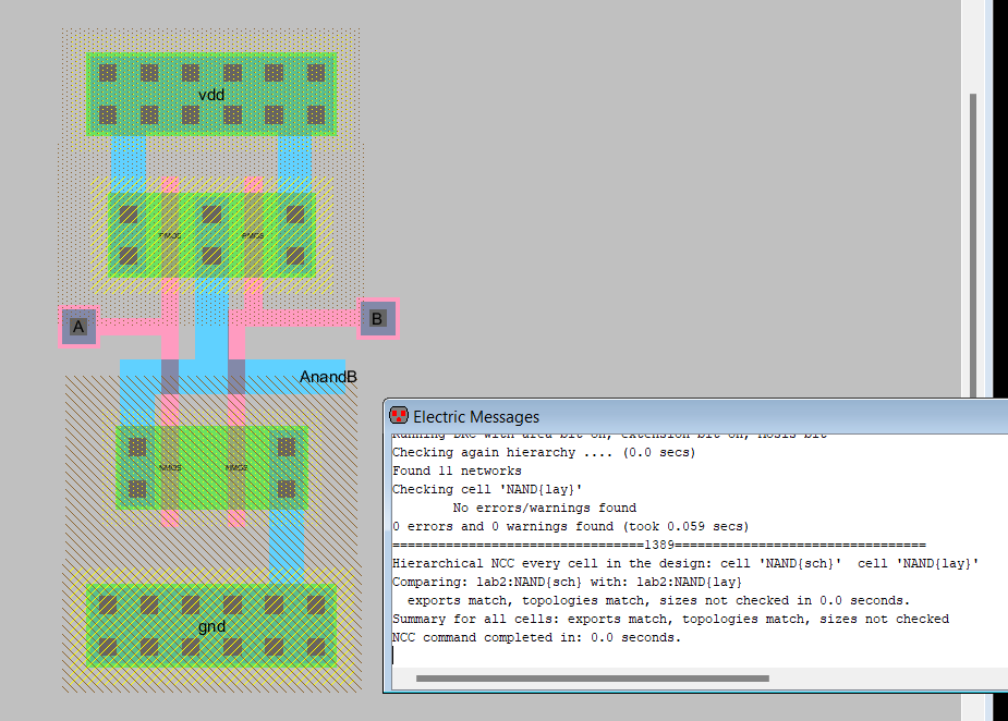
Figure 2: The NAND gate layout.
Figure 3 shows the LTSpice simulation of the NAND gate and the DRC check.
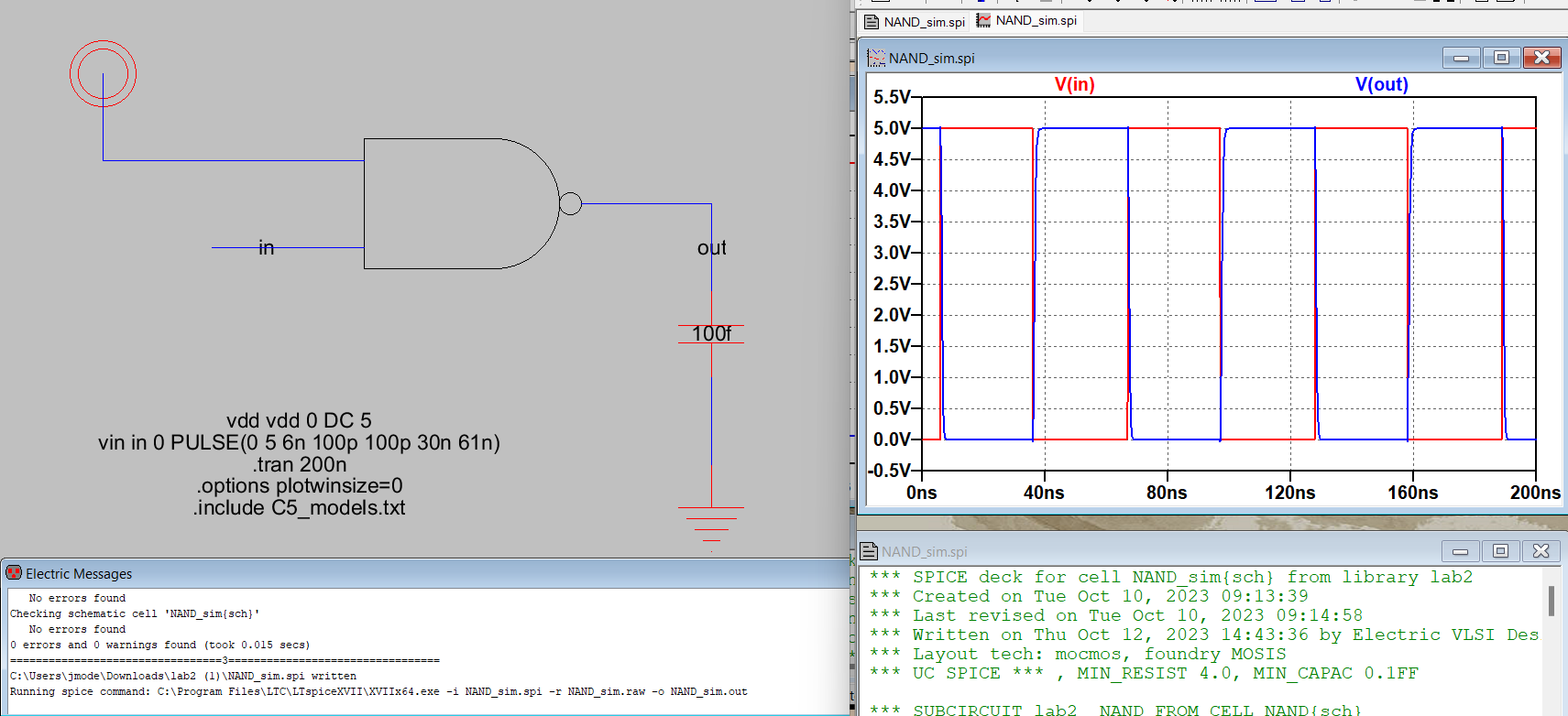
Figure 3: NAND gate simulation.
Figure 4 shows the NOR gate schematic and DRC check.
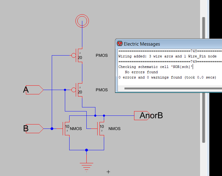
Figure 4: NOR gate schematic.
Figure 5 shows the NOR layout and DRC and NCC check.
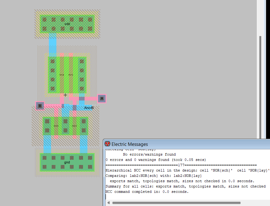
Figure 5: NOR gate layout.
Figure 6 shows the simulation of the NOR gate symbol performed using LTSpice.
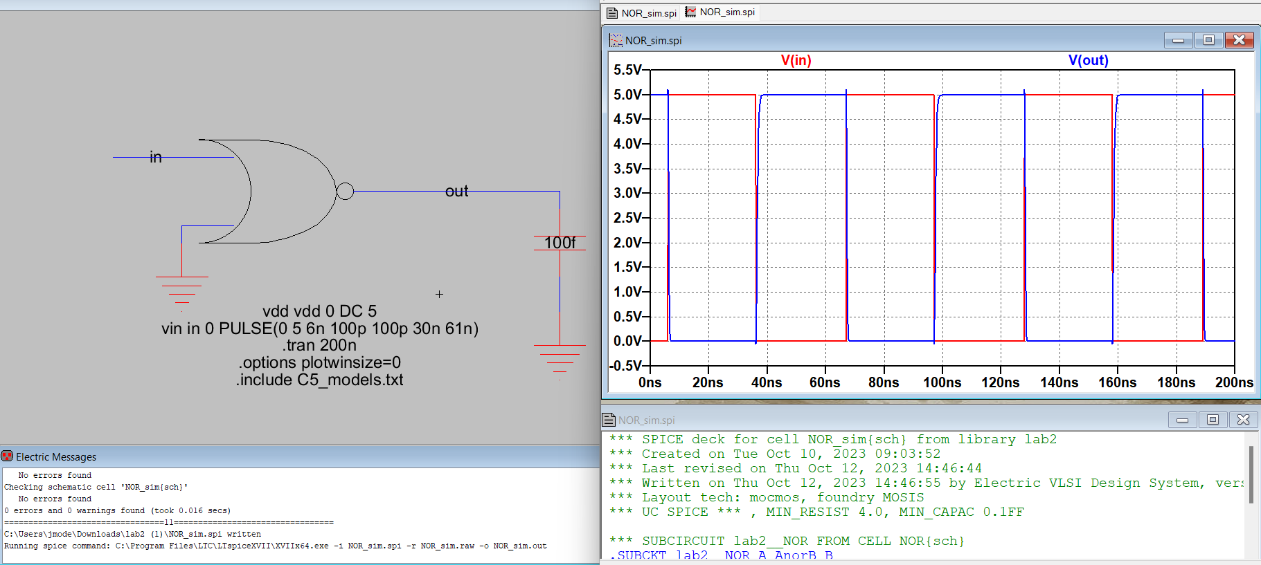
Figure 6: NOR gate simulation.
Figure 7 shows the XOR schematic and XOR icon, as well as the DRC check.
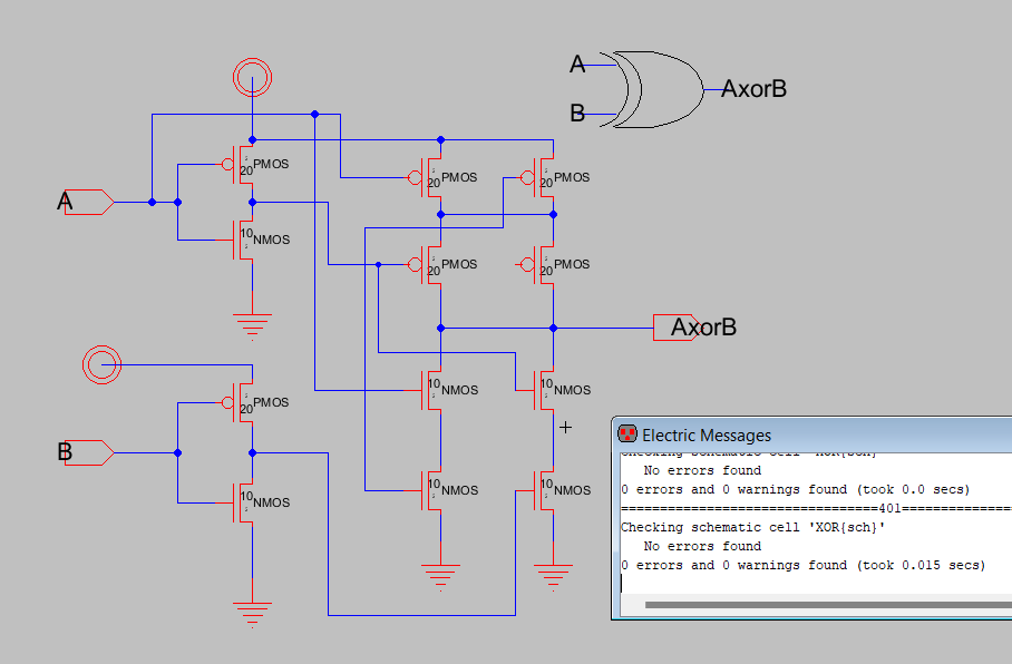
Figure 7: XOR gate schematic.
Figure 8 shows the layout of the XOR gate and the DRC and NCC check.
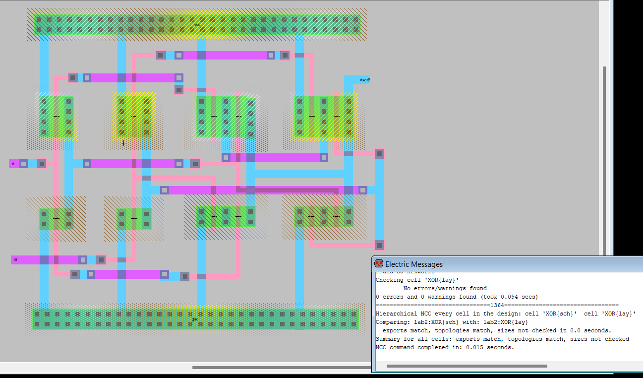
Figure 8 : XOR gate layout.
Figure 9 shows the schematic for the Full Adder and the DRC check.
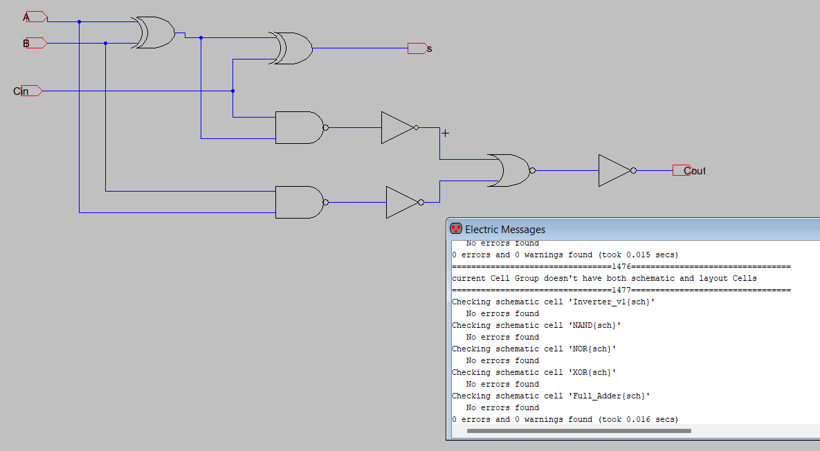
Figure 9: Full Adder schematic.
Figure 10 shows the Full Adder icon for the LTSpice simulation and the DRC check.
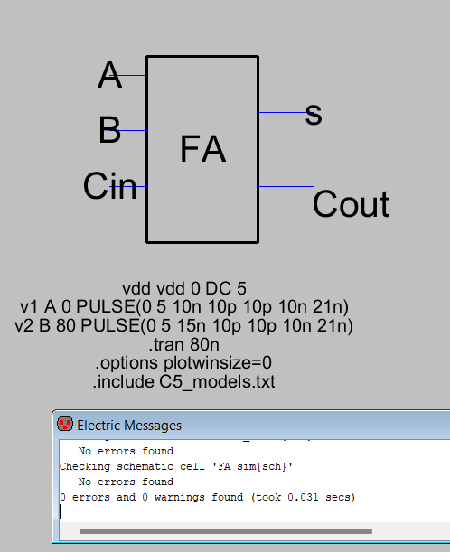
Figure 10: Full Adder icon for simulation.
Figure 11 shows the Full Adder voltages measured at points a, b, s, and cout. Cin was connected to ground.
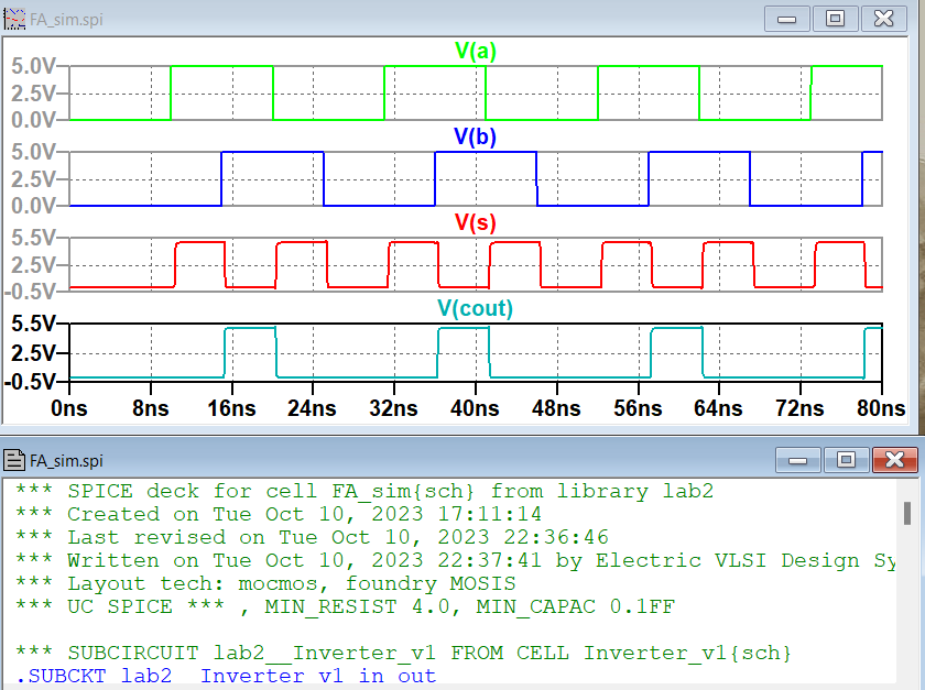
Figure 11: Full Adder simulation when Cin is connected to ground.
Figure 12 shows the Full Adder voltages measured at points a, b, s, and cout. Cin was connected to vdd.
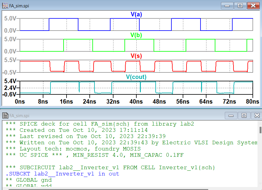
Figure 12: Full Adder simulation when Cin is connected to vdd.
Figure 13 shows the Full Adder layout and the DRC and NCC checks.
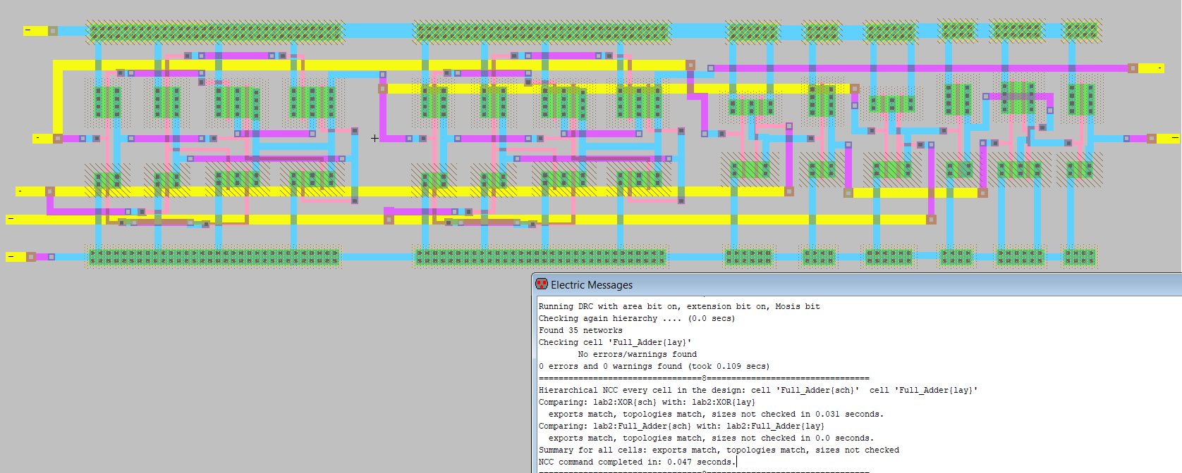
Figure 13: Full Adder layout.
5. Discussion
I had difficulty with the PMOS and NMOS models exporting to LTSpice, as I kept getting an error that the models were not found.
The problem was that I had the schematic, layout, and simulation under the same cell group.
When I moved the simulation to a different cell group, the NMOS and PMOS models exported correctly.
Laying out the XOR gate and the Full Adder were both tricky to get the spacing correct and eliminate DRC errors.
This lab was also good practice for editing icons and making difficult shapes for each gate.
Correctly laying out the Full Adder gives me confidence for the layouts in the next labs that are more complex.