CE338 Digital VLSI Design Lab 2023 Fall
Lab 5
Name: Jesse Moder
Email:
jmmoder@fortlewis.edu
1. The Inverter
2. Introduction
The objective of this tutorial was to layout and simulate an inverter
using Electric VLSI and to simulate the inverter using LTSpice. An
inverter is a low power,
high speed logic gate made of an NMOS and PMOS transistor.
3. Materials and Methods
Electric
VLSI was used to constrcut schematic and layout views of a 20/10 CMOS
inverter. A 100/50 CMOS inverter was constructed using the spice
multiplier tool
and a layout was made using 5 PMOS and 5 NMOS transistors. The 20/10
and 100/50 inverters were connected to 100fF, 1pF, and 10pF capacitors
and were simulated using LTSpice.
DRC and NCC checks were performed to ensure the inverter design passed the design rules.
4. Results
Task 1.
Figure 1 shows the schematic view of the 20/10 inverter created using VLSI.
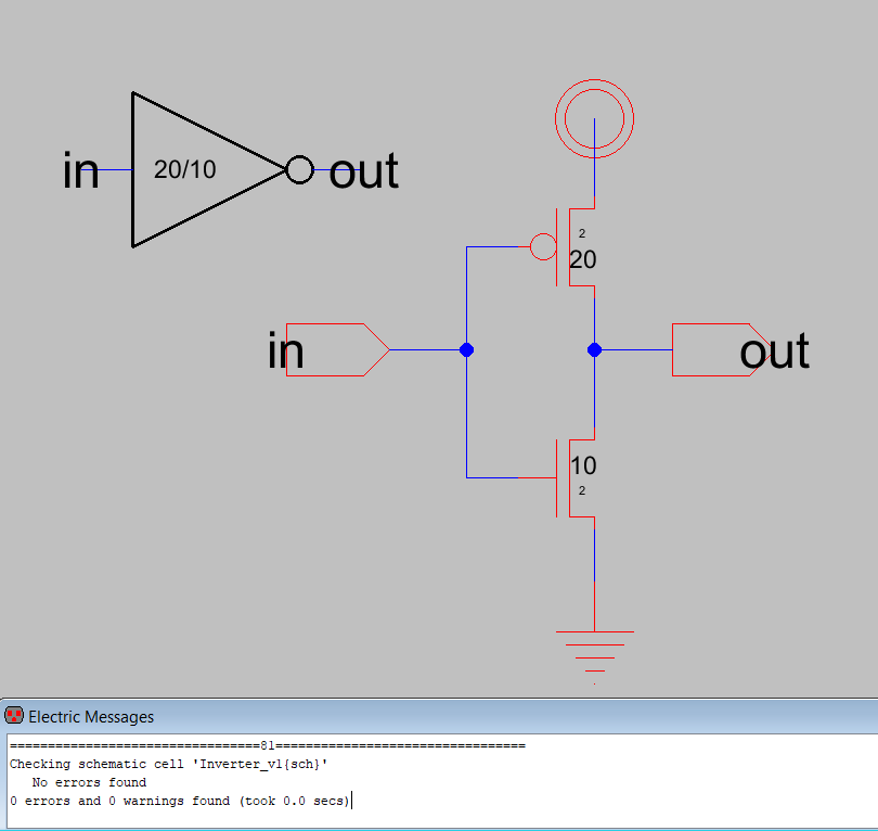
Figure 1: Schematic view of the 20/10 inverter.
Figure 2 shows the LTSpice simulation of the 20/10 inverter.
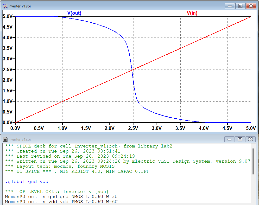
Figure 2: LTSpice simulation of the 20/10 inverter.
Task 2.
Figure 3 shows the layout view of the inverter created in Electric VLSI.
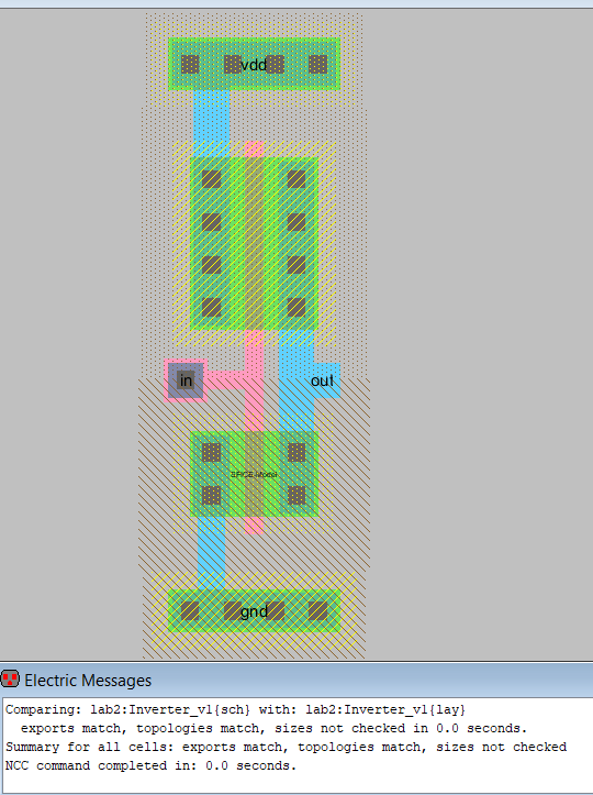
Figure 3: The layout view of the inverter.
Task 3.
Figure 4 shows the schematic of the 100/50 inverter created in Electric VLSI.
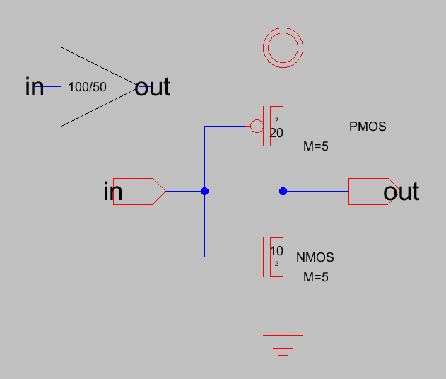
Figure 4: The schematic of the 100/50 inverter.
Figure 5 shows the layout of the 100/50 inverter created in Electric VLSI.
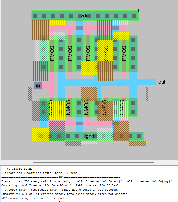
Figure 5: The layout of the 100/50 inverter.
Task 4.
Figure 6 is the 20/10 inverter connected to a 100 fF capacitor and the LTSpice simulation.
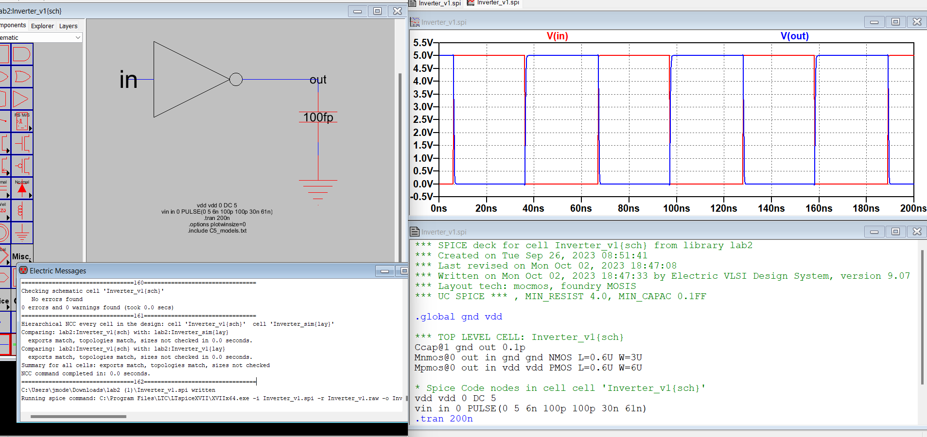
Figure 6: The 20/10 inverter connected to a 100 fF capacitor and the LTSpice simulation.
Figure 7 shows the 20/10 inverter connected to a 1 pF capacitor and the LTSpice simulation.
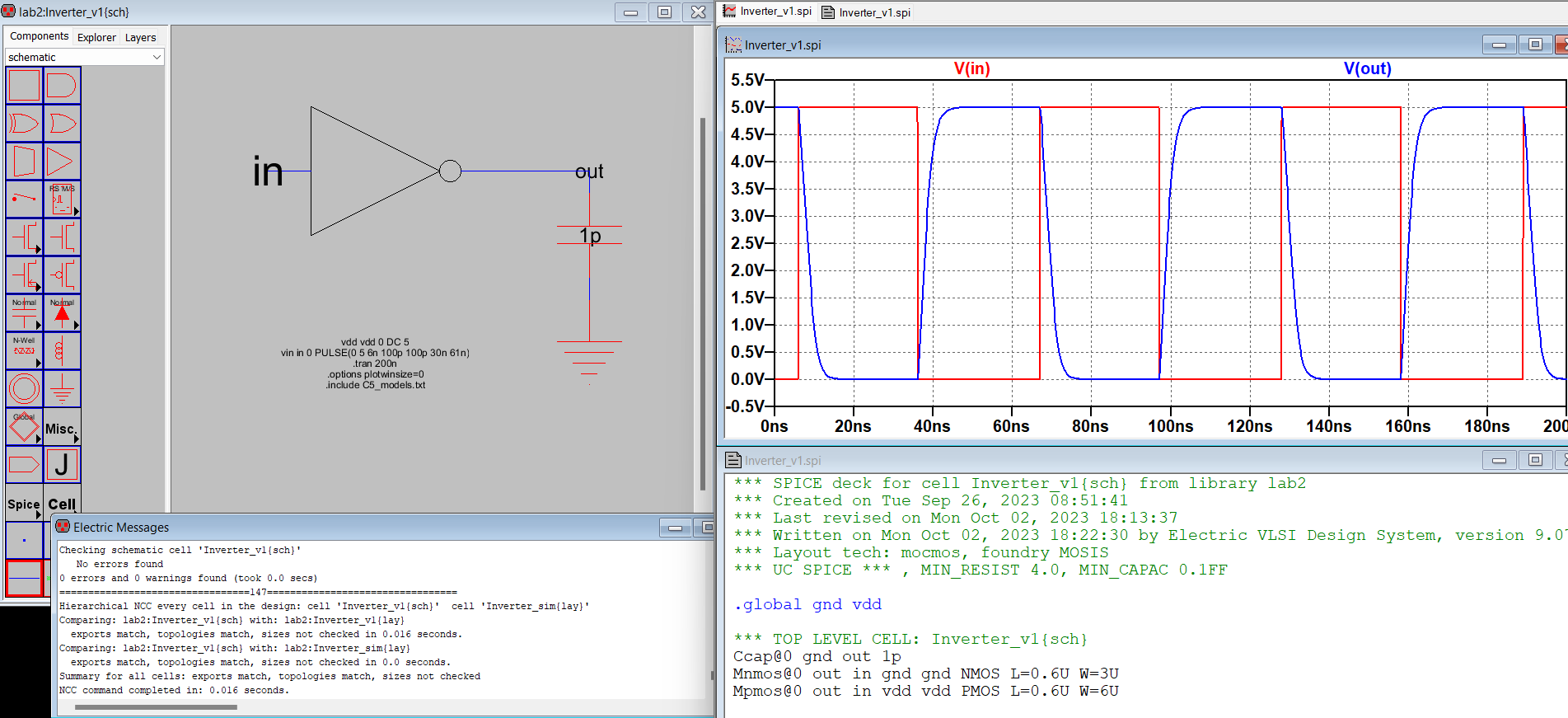
Figure 7: The 20/10 inverter connected to a 1 pF capacitor and the LTSpice simulation.
Figure 8 shows the 20/10 inverter connected to a 10 pF capacitor and the LTSpice simulation.
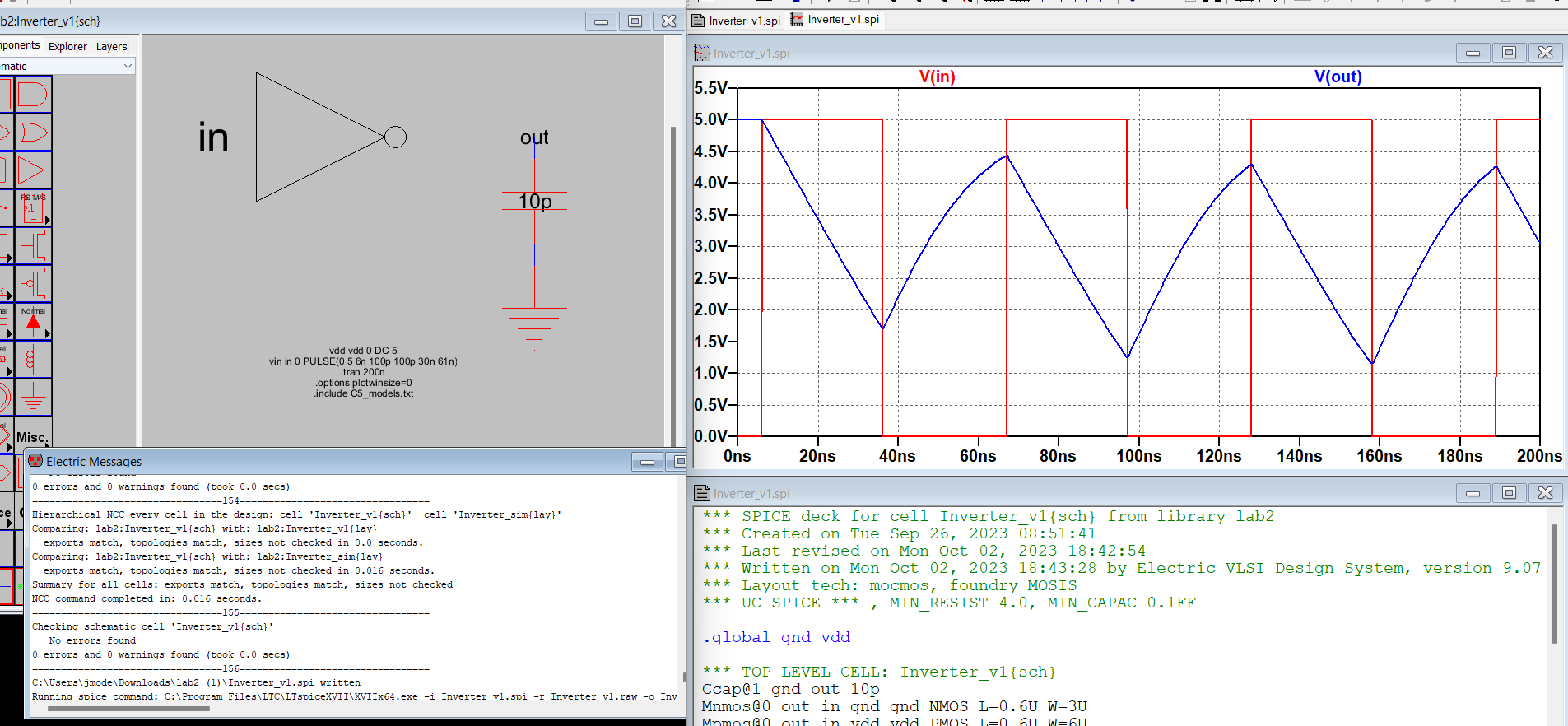
Figure 8: The 20/10 inverter connected to a 10 pF capacitor and the LTSpice simulation.
Figure 9 shows the 100/50 inverter connected to a 100 fF capacitor and the LTSpice simulation.
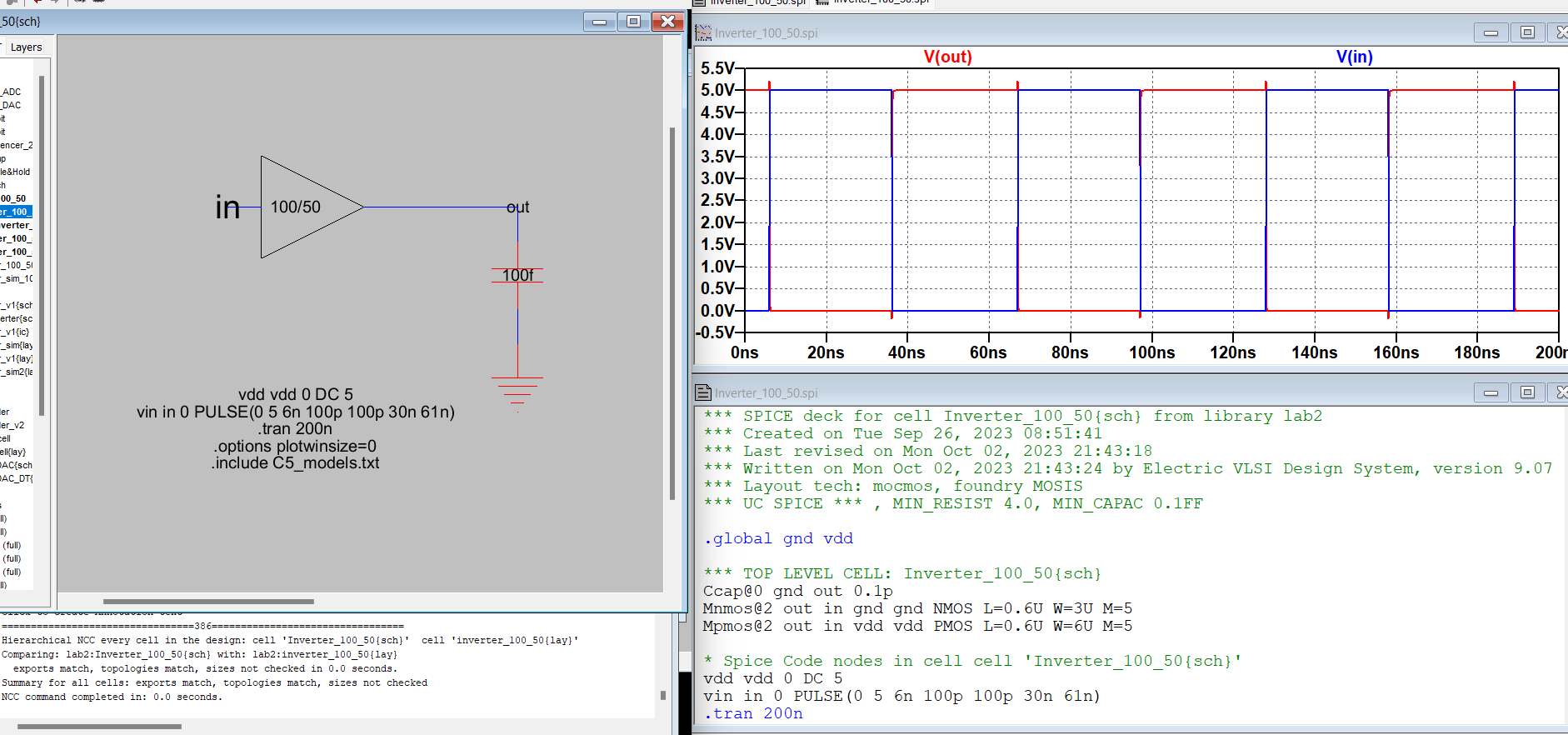
Figure 9: The 100/50 inverter connected to a 100 fF capacitor and the LTSpice simulation.
Figure 10 is the 100/50 inverter connected to a 1 pF capacitor and the LTSpice simulation.
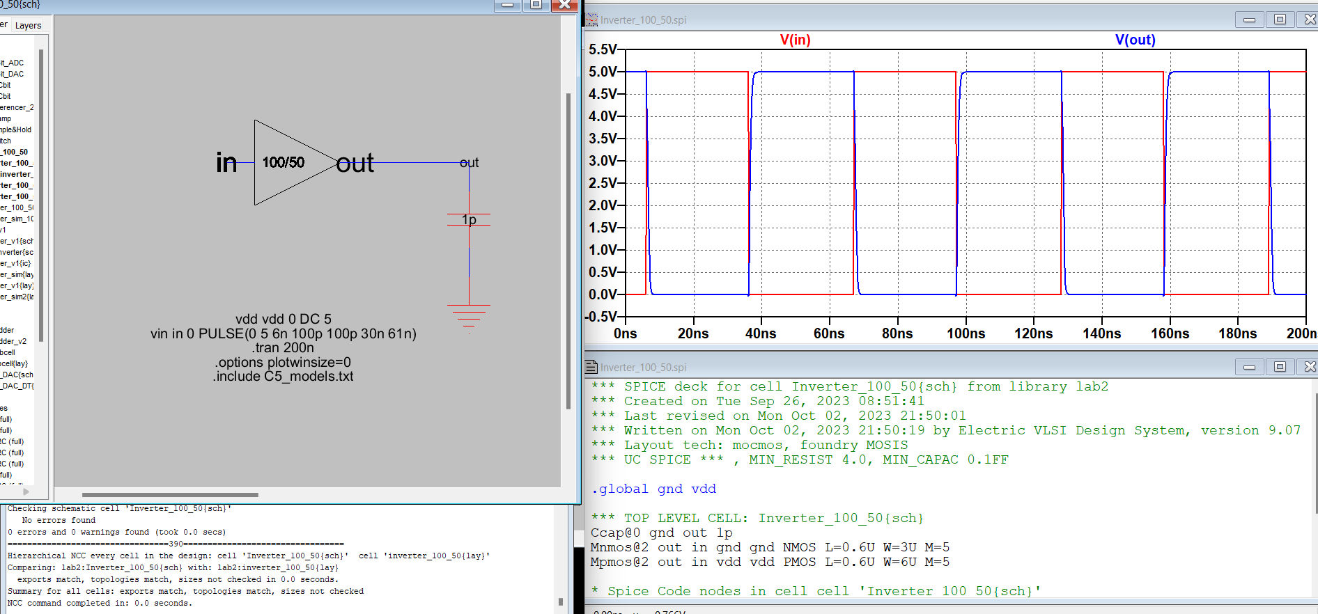
Figure 10: The 100/50 inverter connected to a 1 pF capacitor and the LTSpice simulation.
Figure 11 shows the 100/50 inverter connected to a 10 pF capacitor and the LTSpice simulation.
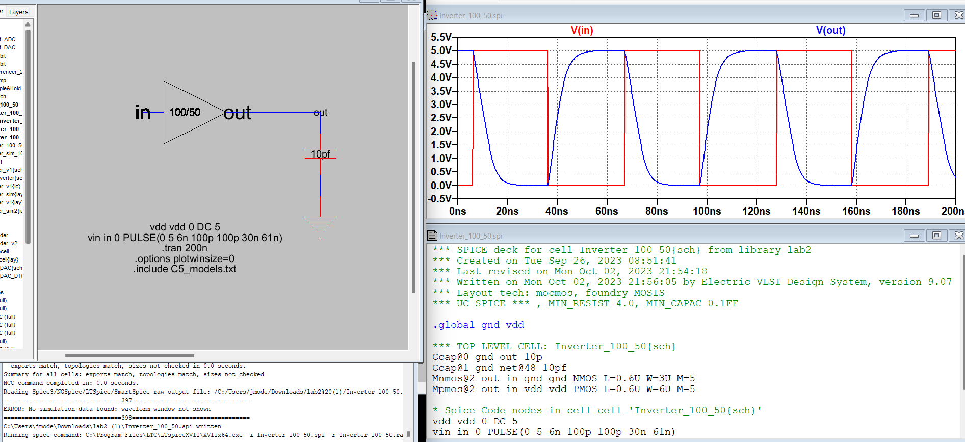
Figure 11: The 100/50 inverter connected to a 10 pF capacitor and the LTSpice simulation.
5. Discussion
This tutorial demonstrated how to build and simulate an inverter
using Electric VLSI and LTSpice. By combining more PMOS and NMOS
transistors, a larger inverter can be created, which reduces the delay
and increases the driving capacity of the system. The 20/10 inverter
was unable to drive the 10 pF capacitor, while the 100/50 inverter was
able to drive the 10 pF capacitor. Learning how to construct parallel
PMOS and NMOS transistors to drive a capacitor was useful to design an
inverter for specific applications in the future.