CE338 Digital VLSI Design Lab 2023 Fall
Lab 4 MOSFETs and IV Curves
Name: Jesse Moder
Email:
jmmoder@fortlewis.edu
1. MOSFETs and IV Curves
2. Introduction
The objectives of this lab were to:
a. be able to build MOSFETs in Electric.
b. be able to run simulations to analyse the IV curves of the MOSFETs.
MOSFETs are low power, high
speed transistors that are used for switching or amplifying signals.
IDS, the current from drain to source, is related to the voltage from
drain to source VDS.
Increases in VDS cause an approximately linear increase in IDS until
VDS nears the saturation voltage. At this point, an increase in VDS
causes a small increase in IDS as the depletion region of the
P-N juntction shrinks. At a high enough voltage, the depletion region
breaks down and IDS increases rapidly with an increase of VDS.
3. Materials and Methods
Electric VLSI was used to constrcut schematic and layout views of an
NMOS and PMOS transistor. DRC and NCC checks were performed to ensure
the transistor design
passed the design rules. The parameters of the circuit were defined in
both the schematic and layout of the NMOS and PMOS transistors. To test
if the transistors were
assembled correctly, the schematic and layouts were exported to LTSpice
for simulation. IDS vs VDS was simulated for each circuit.
4. Results
Figure 1 shows the layout view of the NMOS transistor. Electric VLSI components were selected to build the transistor.
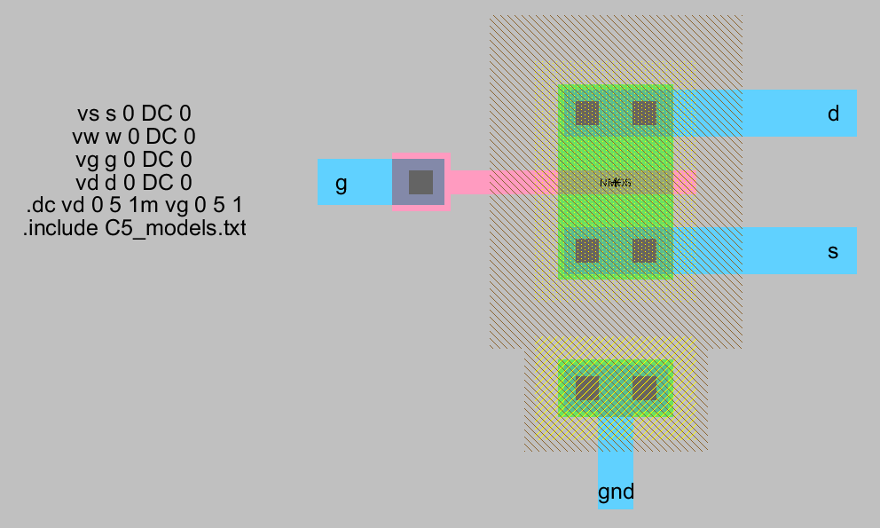
Figure 1: Layout view of the NMOS transistor.
Figure 2 shows the simulated NMOS current IDS as the voltage VDS increases.
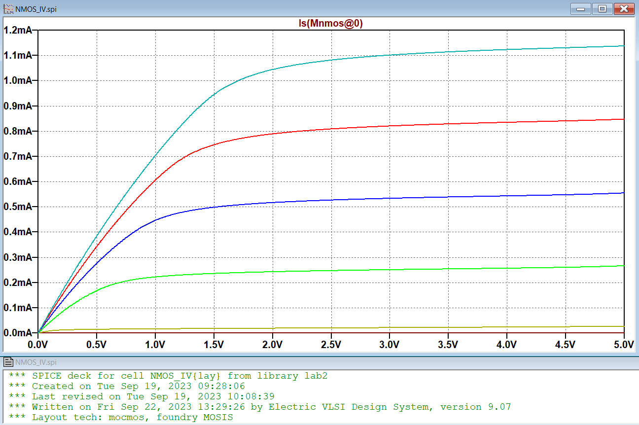
Figure 2: NMOS layout
LTSpice simulation of the current from drain to source as the voltage
from drain to source increases from 0 to 5 V.
Figure 3 is the layout of the PMOS transistor constructed using Electric VLSI.
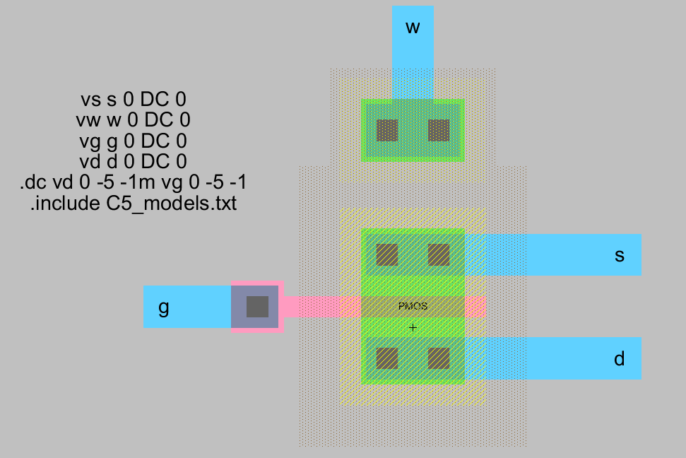
Figure 3: Layout view of the PMOS transistor.
Figure 4 shows the simulated PMOS current IDS as the voltage VDS decreases.
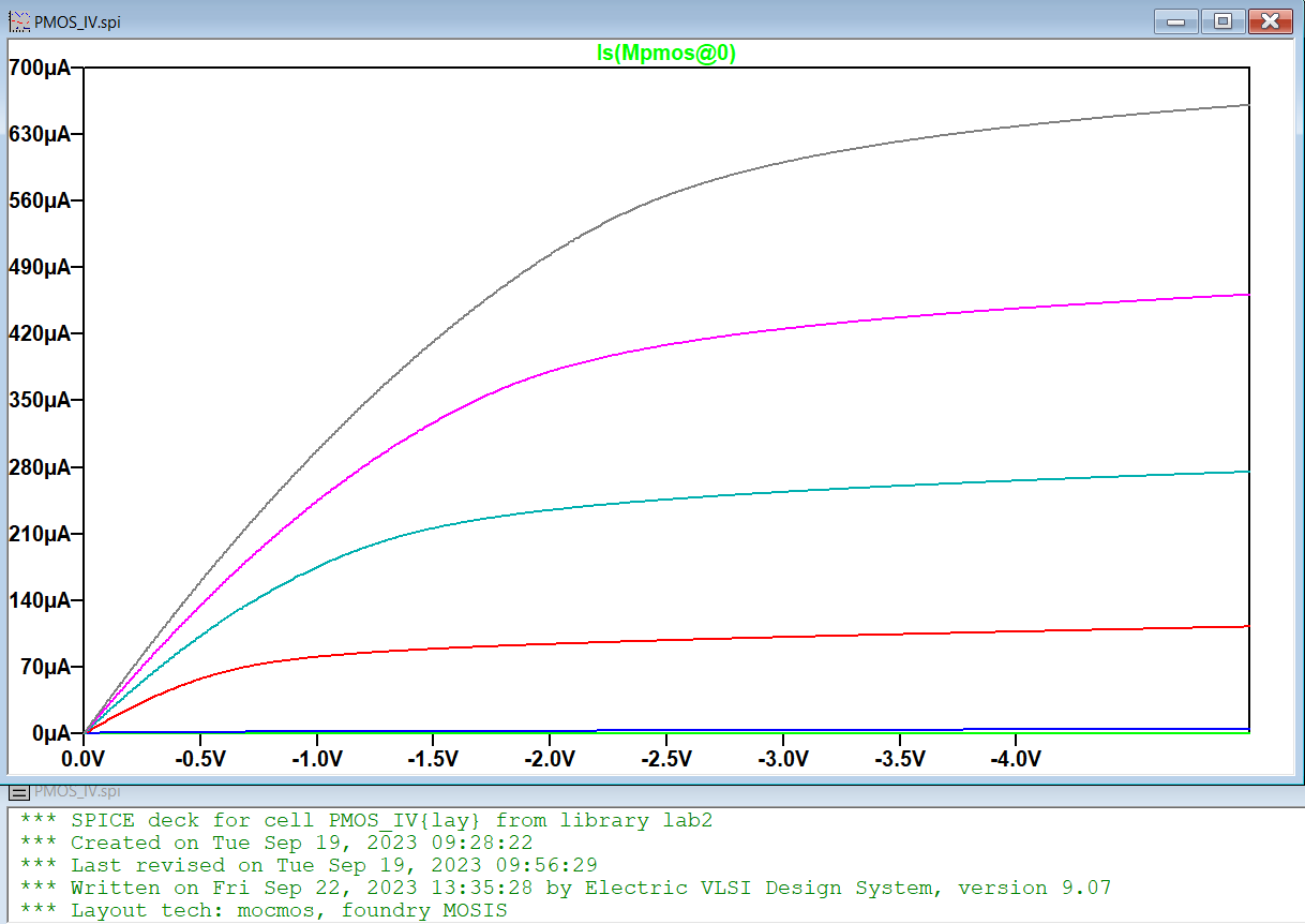
Figure 4: PMOS layout LTSpice simulation of the current from drain to source as the voltage from drain to source decreases from 0 to -5 V.
Figure 5 is the schematic of the NMOS transistor constructed using Electric VLSI.
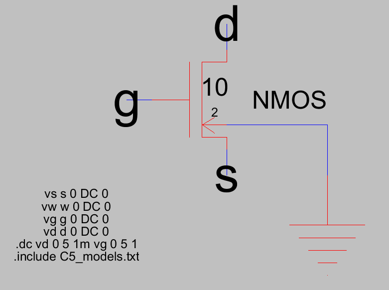
Figure 5: Completed schematic view of the NMOS transistor.
Figure 6 shows the simulated NMOS current IDS as the voltage VDS increases.
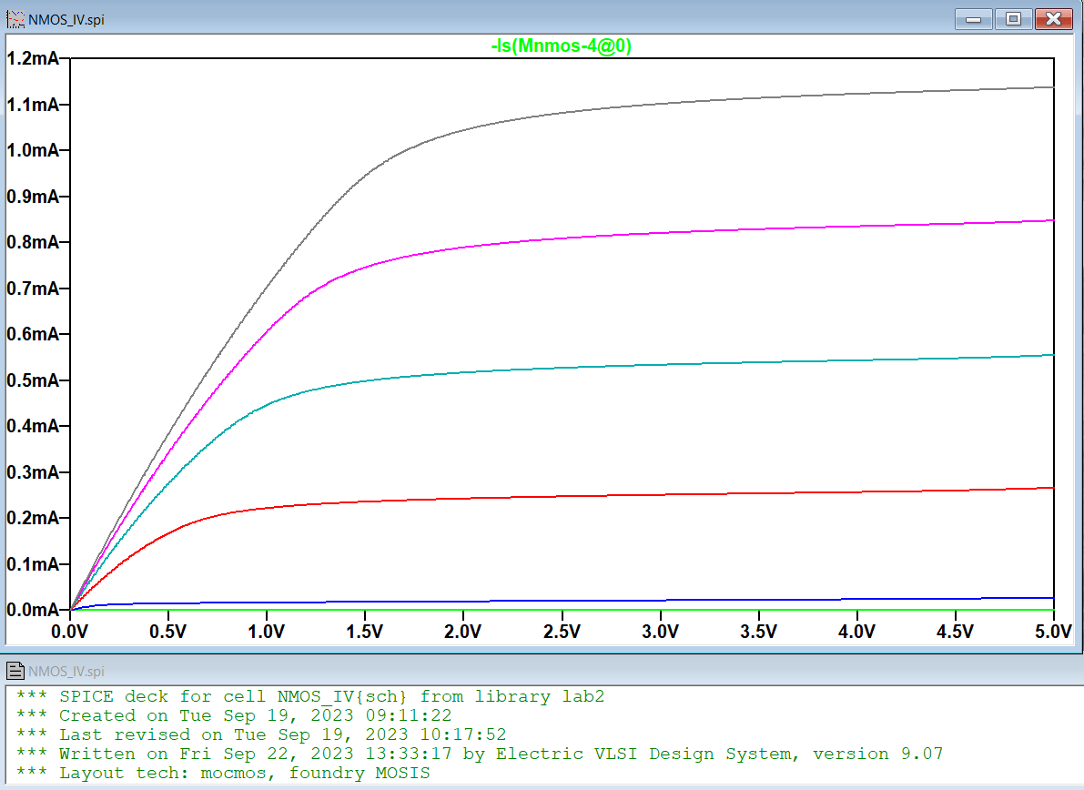
Figure 6: NMOS schematic LTSpice simulation of the current from drain to source as the voltage from drain to source increases from 0 to 5 V.
Figure 7 is the schematic of the PMOS transistor constructed using Electric VLSI.

Figure 7: Completed schematic view of the PMOS transistor.
Figure 8 shows the simulated PMOS current IDS as the voltage VDS decreases.
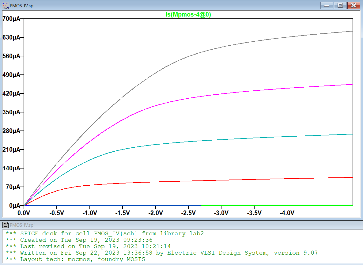
Figure 8: PMOS schematic LTSpice simulation of the current from drain to source as the voltage from drain to source decreases from 0 to -5 V.
Figure 9 shows the NCC check for the PMOS and NMOS schematics and layouts.
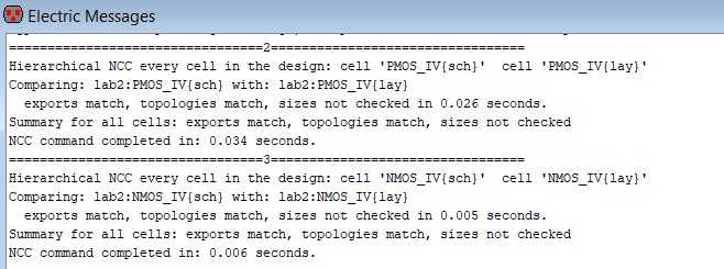
Figure 9: NCC check passed for the NMOS and PMOS schematics and layouts.
5. Discussion
The simulation plots matched what was expected. 0 V drain to source
voltage produced no current, and 1 V produced a tiny amount of current.
Each increase in the magnitude of VDS caused an increase in IDS. IDS
rose more quickly when voltage is first applied but levels out when it
nears the
saturation voltage of the transistor as the depletion region becomes smaller.